Selecting the right Printed Circuit Board (PCB) material is a foundational decision that directly governs signal integrity, especially in high-speed digital and high-frequency RF applications. The electrical properties of a PCB’s dielectric material, primarily its Dielectric Constant (Dk) and Dissipation Factor (Df), determine how fast a signal travels, how much energy it loses, and whether its characteristic impedance is stable. Making an informed choice prevents issues like signal attenuation, timing errors, and reflections, ensuring the final product functions reliably and meets performance specifications.
In the early days of electronics, the PCB substrate was often viewed as simple mechanical scaffolding, a non-conductive plane to hold and connect components. However, as clock speeds have surged into the multi-gigahertz range, this perception has become dangerously outdated. At high frequencies, the PCB material is no longer a passive bystander; it becomes an active and critical component in the circuit. Every trace on the board acts as a transmission line, and the dielectric material it’s embedded in profoundly influences its behavior. Ignoring the impact of the substrate is a direct path to signal integrity nightmares, leading to failed prototypes, costly redesigns, and unreliable end-products.
Table of Contents
- The Foundational Properties: Why Dk and Df Reign Supreme
- Beyond Dk and Df: Secondary Factors That Can Make or Break a Design
- A Practical Guide to Selecting PCB Materials for Signal Integrity
- Conclusion: A Strategic Decision Balancing Performance, Cost, and Reliability
The Foundational Properties: Why Dk and Df Reign Supreme
When engineers discuss PCB materials for signal integrity, two parameters invariably dominate the conversation: the Dielectric Constant (Dk) and the Dissipation Factor (Df). These two properties of the laminate material are the primary determinants of electrical performance for high-frequency signals. Understanding their individual and combined impact is the first step toward making an intelligent material choice.
What is the Dielectric Constant (Dk) and How Does It Affect Signals?
The Dielectric Constant (Dk), also known as relative permittivity (εr), is a measure of a material’s ability to store electrical energy in an electric field. In the context of a PCB, it directly influences two critical signal integrity parameters: characteristic impedance and propagation delay.
- Impact on Characteristic Impedance (Z₀): The impedance of a trace is a function of its physical geometry (trace width, height) and the Dk of the surrounding material. A higher Dk value will result in a lower impedance for the same geometry. For designers, this means that to achieve a target impedance (e.g., 50 ohms), trace dimensions must be precisely calculated based on the material’s Dk. An unstable or incorrect Dk value will lead to impedance mismatches, causing signal reflections, ringing, and degraded signal quality.
- Impact on Propagation Delay: The Dk also dictates how fast a signal propagates down a trace. The signal velocity is inversely proportional to the square root of the dielectric constant. A material with a higher Dk will slow the signal down, increasing the propagation delay. In high-speed systems where timing is critical (like DDR memory interfaces), even small variations in delay can lead to timing violations and system failure.
Crucially, the Dk of many materials, especially standard FR-4, is not a fixed number. It can vary significantly with frequency. A material might have a Dk of 4.7 at 1 MHz but drop to 4.2 at 3 GHz. For broadband signals containing a wide range of frequencies, this variation causes different frequency components to travel at different speeds, an effect known as dispersion, which distorts the signal waveform. Therefore, for high-speed applications, selecting a material with a stable Dk across the target frequency range is paramount.
What is the Dissipation Factor (Df) and Why is It the Enemy of Signal Strength?
The Dissipation Factor (Df), often called the Loss Tangent (tanδ), quantifies how much of a signal’s energy is absorbed and lost as heat within the dielectric material. While Dk affects timing and impedance, Df directly determines signal attenuation, or dielectric loss. A material with a high Df is “lossy,” acting like a resistor that dampens the signal as it travels.
This effect becomes dramatically more pronounced as frequency increases. A signal might travel across a standard FR-4 board at 100 MHz with negligible loss, but at 5 GHz, the same trace could experience such severe attenuation that the signal becomes unusable at the receiver. This is why Df is a primary concern for any design operating above 1 GHz, including PCIe, USB 3.0, SATA, and RF systems. A low Df material preserves the amplitude of the signal, ensuring it arrives at its destination with enough strength to be correctly interpreted. Choosing a material with a Df that is too high for the operating frequency is one of the most common and costly signal integrity mistakes.
Beyond Dk and Df: Secondary Factors That Can Make or Break a Design
While Dk and Df are the stars of the show, a successful high-speed design requires considering a supporting cast of other material and physical properties. These factors contribute to different forms of signal loss and affect the overall reliability and manufacturability of the board.
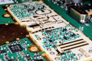
Conductor Loss: Understanding Skin Effect and Copper Surface Roughness
Signal loss isn’t just about the dielectric; the copper traces themselves contribute significantly, especially at high frequencies. This is primarily due to two phenomena:
- Skin Effect: At DC or low frequencies, current flows uniformly through the entire cross-section of a conductor. As frequency increases, electromagnetic effects force the current to concentrate near the outer surface, or “skin,” of the conductor. This effectively reduces the usable cross-sectional area, increasing the trace’s resistance and causing what is known as conductor loss.
- Copper Surface Roughness: To ensure a strong bond between the copper foil and the dielectric laminate, the copper is chemically treated to create a rough, tooth-like surface. At high frequencies where the skin effect is prominent, the signal current is forced to follow this jagged, uneven path. This increases the effective path length compared to a perfectly smooth surface, further elevating the conductor’s resistance and contributing significantly to overall insertion loss. Low-profile and very-low-profile copper foils are available with high-performance laminates to mitigate this effect, but they come at a higher cost.
The Importance of Thermal and Mechanical Stability (Tg, Td, CTE)
The physical reliability of the PCB directly impacts its long-term signal integrity. Key thermal properties include:
- Glass Transition Temperature (Tg): The temperature at which the PCB material transitions from a rigid, glassy state to a softer, rubbery state. A higher Tg indicates better stability during the high temperatures of assembly (soldering).
- Decomposition Temperature (Td): The temperature at which the material chemically decomposes. This should be significantly higher than soldering temperatures.
- Coefficient of Thermal Expansion (CTE): A measure of how much the material expands or contracts with temperature changes. A high CTE, especially in the Z-axis (thickness), can put immense stress on plated through-holes and vias during thermal cycling, potentially leading to barrel cracking and open circuits—a catastrophic failure for signal integrity.
A material with poor thermal stability can delaminate or cause via failures during assembly or operation, creating intermittent or permanent signal path interruptions. Therefore, choosing a material with robust thermal properties is essential for product reliability.
How Moisture Absorption Can Sabotage Performance
PCB laminates are not perfectly impervious; they can absorb moisture from the ambient environment. Water has a very high Dk (around 70) and a high Df. When a PCB material absorbs moisture, its overall Dk and Df values increase. This change can alter trace impedance and increase dielectric loss, causing a design that worked perfectly in a dry lab to fail in a humid field environment. For applications in uncontrolled environments, selecting a material with low moisture absorption is a critical reliability consideration.
A Practical Guide to Selecting PCB Materials for Signal Integrity
With an understanding of the key properties, the selection process becomes a methodical exercise in balancing performance, cost, and manufacturability against the specific requirements of your design.
First, Understand Your Application’s Demands
Before looking at material datasheets, answer these questions about your project:
- What is the maximum signal frequency or fastest signal rise time? This is the single most important factor. Frequencies above 1-3 GHz almost always rule out standard FR-4.
- What are the critical trace lengths? A short trace might tolerate a lossier material, while a long backplane trace will require a low-loss laminate to maintain signal amplitude.
- What is the project budget? High-performance materials can cost 5-10 times more than standard FR-4. The goal is to choose the most cost-effective material that meets the performance requirements, not necessarily the best-performing material available.
- What is the operating environment? Will the device operate in extreme temperatures or high humidity? This will influence requirements for CTE and moisture absorption.
An Overview of PCB Material Categories and Their Trade-offs
PCB laminates can be broadly grouped into tiers based on their performance and cost.
- Standard FR-4: The workhorse of the industry. It’s inexpensive and easy to manufacture. However, it has a relatively high and frequency-dependent Dk and Df, making it unsuitable for applications above ~1-3 GHz. It’s perfect for low-speed digital, power supplies, and analog circuits.
- Mid-Loss and Low-Loss Materials: This category represents the sweet spot for many modern high-speed digital designs (e.g., PCIe Gen 3/4, DDR4). Materials like Megtron 6, Isola FR408HR, or I-Speed have significantly better and more stable Dk/Df properties than standard FR-4. They offer a great balance of performance and cost.
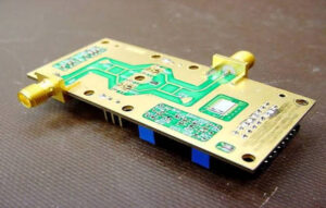
- Ultra-Low Loss (High-Frequency/RF) Materials: This is the premium tier, including materials based on PTFE (like Teflon) and specialized thermoset resins (e.g., Rogers RO4000 series). These laminates offer exceptionally low and stable Dk and Df values, making them essential for microwave and millimeter-wave RF applications (e.g., radar, 5G antennas). However, they are very expensive and can require specialized manufacturing processes.
Material Comparison at a Glance
The following table provides a general comparison of these material categories. Note that specific values vary widely between manufacturers and exact product lines.
| Property | Standard FR-4 | Mid/Low-Loss (e.g., Megtron 6) | Ultra-Low Loss (e.g., Rogers 4350B) |
|---|---|---|---|
| Typical Dk (@ 10 GHz) | ~4.2 – 4.5 (Highly Variable) | ~3.3 – 3.6 (Stable) | ~3.5 – 3.7 (Very Stable) |
| Typical Df (@ 10 GHz) | ~0.020 – 0.025 | ~0.004 – 0.008 | ~0.003 – 0.004 |
| Max Frequency (Rule of Thumb) | < 3 GHz | 3 GHz – 15 GHz | > 15 GHz (up to 40 GHz+) |
| Relative Cost | 1x (Baseline) | 3x – 6x | 5x – 10x+ |
| Key Applications | Low-speed logic, Power, IoT | Servers, Networking, PCIe, DDR4/5 | RF/Microwave, 5G, Automotive Radar |
Conclusion: A Strategic Decision Balancing Performance, Cost, and Reliability
Choosing a PCB material is no longer a trivial task; it is a critical engineering decision that lies at the intersection of electrical performance, mechanical reliability, and budget. By fundamentally controlling impedance, signal speed, and attenuation, the PCB substrate has a direct and profound impact on signal integrity. An inappropriate material choice can render an otherwise excellent circuit design completely non-functional.
The key is to move from a “cost-first” to a “performance-first” mindset during the early stages of design. By carefully analyzing the frequency and timing requirements of your signals, you can select the most cost-effective material tier that reliably meets those needs. Investing in a suitable low-loss laminate upfront is far cheaper than troubleshooting signal integrity failures in a finished product or undertaking a full-scale redesign. In the world of high-speed electronics, the foundation you build upon matters, and that foundation is the PCB material itself.
PCB material selection, signal integrity, high-speed PCB design, dielectric constant, dissipation factor, loss tangent, PCB laminate materials, signal loss in PCB, impedance control, skin effect, PCB surface roughness, FR-4, Rogers PCB material