High-frequency PCB fabrication is different from standard PCB manufacturing because the circuit board must control signal loss, impedance, dielectric behavior, copper roughness, and transmission-line performance at RF or microwave frequencies. A standard PCB is mainly designed to provide reliable electrical interconnection, while a high-frequency circuit board often becomes part of the signal transmission structure itself.
In standard PCB manufacturing, material selection, trace geometry, copper thickness, and layer stackup are important. In high frequency PCB fabrication, these factors become even more critical because small variations can affect insertion loss, impedance matching, phase stability, return loss, and overall RF performance.
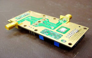
For applications such as radar systems, 5G communication modules, antennas, RF amplifiers, microwave circuits, satellite communication equipment, and high-frequency test devices, working with a manufacturer experienced in high-frequency RF PCB fabrication can help reduce design-to-production risk.
What Is a High-Frequency PCB?
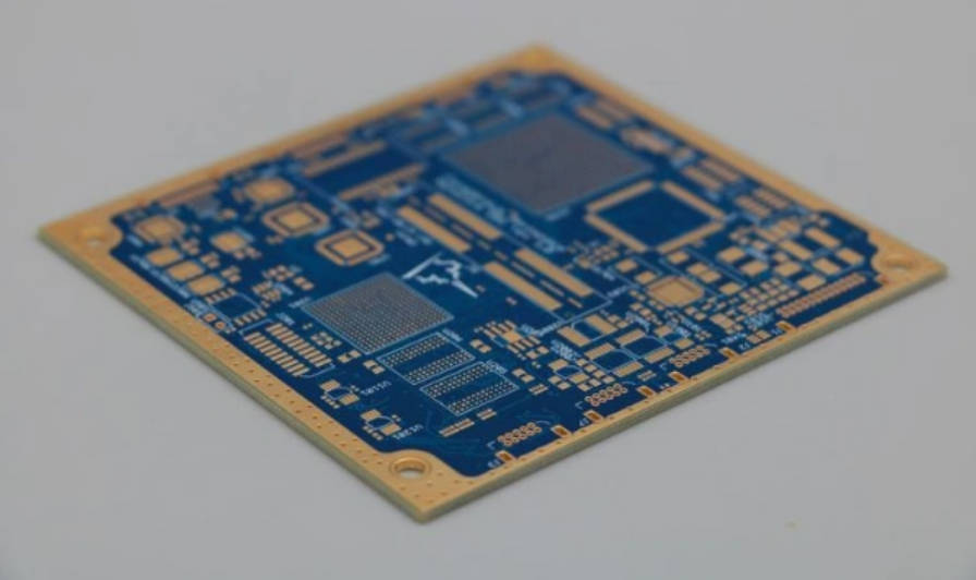
A high-frequency PCB is a printed circuit board designed to transmit high-frequency signals with controlled loss, stable impedance, and predictable electromagnetic behavior. These boards are commonly used in RF, microwave, wireless communication, radar, antenna, satellite, and high-speed signal applications.
Unlike standard PCBs, high-frequency PCBs require more attention to the electrical characteristics of the substrate and copper structure. The board material, dielectric thickness, copper profile, stackup, trace width, spacing, via structure, and surface finish can all influence performance.
A high-frequency PCB is not simply a standard PCB made with a different material. It is a board where material properties, stackup design, and fabrication control must work together to support signal integrity.
What Is Standard PCB Manufacturing?
Standard PCB manufacturing refers to the fabrication of general printed circuit boards used in consumer electronics, industrial control systems, power supplies, LED products, automotive electronics, household appliances, and many other applications.
Standard PCBs are often manufactured with FR4 or similar materials. The main manufacturing priorities usually include:
- Mechanical reliability
- Electrical continuity
- Solderability
- Dimensional accuracy
- Layer registration
- Cost control
- Production efficiency
- Assembly compatibility
For many low-frequency or moderate-speed circuits, standard PCB fabrication is sufficient. However, when the signal frequency increases and the board begins to behave like a transmission medium, standard PCB manufacturing methods may not provide enough control over loss, impedance, and signal behavior.
High-Frequency PCB Fabrication vs Standard PCB Manufacturing
The most important difference is that high-frequency PCBs must preserve electrical performance at high frequencies, while standard PCBs mainly focus on connectivity and general reliability.
| Comparison Item | Standard PCB Manufacturing | High-Frequency PCB Fabrication |
| Main goal | Reliable electrical connection | Controlled RF/microwave signal transmission |
| Common materials | FR4, standard laminates | Low-loss RF materials, PTFE, ceramic-filled PTFE, Rogers-type laminates, low-loss substrates |
| Key electrical concerns | Continuity, insulation, basic impedance when required | Dk, Df, insertion loss, return loss, phase stability, impedance control |
| Stackup focus | Routing, mechanical structure, cost | Transmission-line structure, dielectric thickness, reference planes, impedance |
| Copper consideration | Copper weight and current capacity | Copper roughness, conductor loss, plating thickness, trace edge quality |
| Tolerance sensitivity | Moderate for many applications | High, especially for RF traces and dielectric thickness |
| Lamination requirement | Standard process control | More careful control of pressure, temperature, bonding, and dielectric stability |
| Testing focus | Open/short test, dimensional inspection, standard quality checks | Electrical test plus impedance verification and closer process review when required |
| Typical applications | Industrial electronics, consumer products, power boards | Radar, antennas, RF modules, microwave circuits, satellite communication, 5G devices |
The practical difference is this: a standard PCB can pass electrical continuity testing but still fail in an RF system if material loss, impedance, or stackup behavior is not properly controlled.
Why the Difference Matters to Engineers and Buyers
For a purchasing team, the difference between standard PCB and high-frequency PCB fabrication affects cost, lead time, material selection, supplier qualification, and project risk.
For an engineer, the difference affects whether the actual fabricated board will match simulation and design expectations. A circuit may work in simulation but perform poorly after fabrication if the real PCB has different dielectric behavior, trace geometry, copper roughness, or stackup thickness.
This matters because high-frequency boards are used in systems where performance margins may be narrow. Poor PCB fabrication control can cause:
- Excessive insertion loss
- Impedance mismatch
- Signal reflection
- Reduced antenna efficiency
- Lower RF output power
- Increased noise
- Poor phase consistency
- Unstable production repeatability
- Prototype failure or redesign
For B2B projects, these problems can delay product development, increase testing cost, and create uncertainty before mass production.
1. Material Selection Is More Critical in High-Frequency PCB Fabrication
In standard PCB manufacturing, FR4 is widely used because it is cost-effective, easy to process, and suitable for many general applications. However, in high-frequency applications, material properties must be selected more carefully.
The most important material factors include:
| Material Factor | Why It Matters in High-Frequency PCB Fabrication |
| Dielectric constant, or Dk | Affects impedance, signal speed, wavelength, and phase behavior |
| Dissipation factor, or Df | Affects dielectric loss and insertion loss |
| Dk stability | Helps maintain predictable performance across frequency and temperature |
| Moisture absorption | Can affect dielectric performance and reliability |
| Thermal stability | Important for RF power and harsh environments |
| Copper type | Influences conductor loss and manufacturing behavior |
| Thickness tolerance | Affects impedance and transmission-line performance |
Standard FR4 may be acceptable for some moderate-frequency or cost-sensitive designs. However, for microwave circuits, precision RF filters, antenna feed networks, radar boards, or low-loss communication modules, specialized RF materials are often preferred.
Mars-PCB supports customers working with high-frequency board requirements through its high-frequency PCB manufacturing service, where material selection and fabrication requirements can be reviewed based on the application.
2. Dielectric Loss and Insertion Loss Become Key Manufacturing Concerns
In many standard PCBs, small dielectric loss is not the main design limitation. In high-frequency PCBs, dielectric loss can directly affect system performance.
Insertion loss is the signal power lost as a signal travels through the PCB transmission path. It can come from multiple sources:
| Loss Source | Description |
| Dielectric loss | Energy absorbed by the substrate material |
| Conductor loss | Loss caused by copper resistance and current distribution |
| Copper roughness loss | Additional conductor loss from rough copper surfaces |
| Reflection loss | Loss caused by impedance discontinuity |
| Radiation loss | Energy radiated from poorly controlled structures |
| Via transition loss | Loss from vias, pads, stubs, and layer changes |
High-frequency PCB fabrication must control both material loss and manufacturing-related loss, because both can influence RF and microwave circuit performance.
This is one reason why high-frequency PCBs often require closer collaboration between the PCB designer and manufacturer before production begins.
3. Controlled Impedance Is Usually More Demanding
Controlled impedance is important in both high-speed digital boards and RF boards, but the reason and sensitivity can be different.
In a high-frequency circuit board, traces often function as transmission lines. Their impedance is determined by trace width, copper thickness, dielectric thickness, Dk, spacing, and reference plane structure. If these values shift during fabrication, the final impedance may deviate from the design target.
Important controlled impedance factors include:
- Trace width tolerance
- Trace spacing tolerance
- Copper thickness after plating
- Dielectric thickness tolerance
- Etching compensation
- Dk value and tolerance
- Reference plane location
- Surface finish thickness
- Via and pad transitions
In standard PCB manufacturing, impedance control may be required only for selected high-speed interfaces. In RF PCB fabrication, impedance behavior may affect almost every critical signal path.
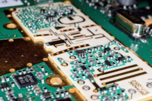
4. Copper Roughness Has Greater Impact at High Frequencies
At high frequencies, current tends to flow near the surface of the conductor. This is known as the skin effect. Because of this, copper surface roughness becomes more important in high-frequency circuits than in many standard PCB applications.
Rougher copper can improve adhesion, but it may also increase conductor loss. Smoother copper can reduce loss in RF and microwave circuits, but it must still support reliable bonding and fabrication.
| Copper Consideration | Standard PCB Manufacturing | High-Frequency PCB Fabrication |
| Main concern | Copper thickness, current capacity, etching quality | Copper roughness, conductor loss, trace accuracy, plating consistency |
| Loss sensitivity | Lower in many low-frequency circuits | Higher at RF and microwave frequencies |
| Selection basis | Cost, availability, electrical current | Loss budget, adhesion, manufacturability, RF performance |
| Engineering review | Often basic | Often needs review with material and stackup |
In high-frequency PCB fabrication, copper is not only a conductor. Its surface profile can become part of the signal-loss equation.
5. Stackup Design Is More Than a Layer Arrangement
For standard PCBs, stackup design usually considers routing density, power distribution, mechanical thickness, and cost. For high-frequency PCBs, stackup design must also support controlled transmission-line structures.
Common high-frequency transmission-line structures include:
- Microstrip
- Stripline
- Grounded coplanar waveguide
- Differential transmission lines
- Antenna feed structures
- RF power paths
A high-frequency PCB stackup should define:
- RF signal layers
- Ground reference layers
- Dielectric material and thickness
- Copper thickness
- Impedance values
- Isolation between RF and digital circuits
- Symmetry for lamination control
- Hybrid material compatibility, if used
If the stackup is not clearly defined, the manufacturer may need to make assumptions. In RF and microwave applications, assumptions can create performance risk.
6. Line Width, Line Spacing, and Etching Tolerance Are More Sensitive
In standard PCB manufacturing, small line width variation may not always affect product performance significantly. In high-frequency PCB fabrication, trace geometry is directly connected to impedance and RF behavior.
Etching tolerance affects:
- Characteristic impedance
- Coupling
- Return loss
- Insertion loss
- Resonant behavior
- Filter response
- Phase matching
For high-frequency boards, the manufacturer may need to apply etching compensation based on copper thickness, trace width, and process capability. Fine RF features may also require more careful panel planning and inspection.
This is especially important for:
- RF filters
- Antenna matching networks
- Microwave couplers
- Power dividers
- Phase-sensitive circuits
- High-frequency test boards
7. Lamination Process Control Is More Complex
High-frequency boards may use materials that behave differently from standard FR4 during lamination. Some RF materials have different thermal expansion, bonding behavior, resin flow, and dimensional stability.
Lamination process control can affect:
- Dielectric thickness
- Bonding quality
- Void formation
- Layer registration
- Warpage
- Impedance stability
- Reliability under thermal stress
Hybrid stackups can be especially challenging because they may combine different materials in one board. For example, a design may use RF material on critical signal layers and FR4 on supporting layers to balance performance and cost. This can be useful, but it requires careful engineering review.
A manufacturer experienced in RF PCB fabrication can help evaluate whether a proposed stackup is practical before production.
8. Via Design and Layer Transitions Need More Attention
Vias are common in standard PCBs, but in high-frequency circuits they can introduce discontinuities. A signal via may create parasitic inductance, capacitance, and unwanted stubs. These effects become more significant as frequency increases.
High-frequency via design should consider:
- Via stub length
- Signal via transitions
- Ground via placement
- Back drilling, if required
- Pad and anti-pad geometry
- Return current path
- Via-to-plane connection quality
- RF launch structures
For microwave circuits, even a short via stub may affect performance in some designs. Designers should review whether critical RF paths can stay on one layer or whether via transitions need special treatment.
9. Testing and Inspection Requirements Are Different
Standard PCB testing often focuses on open/short testing, dimensional inspection, solderability, hole quality, and general reliability. High-frequency PCB fabrication may require additional engineering checks depending on project requirements.
Possible checks include:
| Check Type | Purpose |
| Electrical open/short test | Confirms basic connectivity |
| Impedance testing | Verifies controlled impedance structures |
| Material verification | Confirms specified laminate and thickness |
| Dimensional inspection | Checks trace width, hole size, and board outline |
| Cross-section inspection | Reviews plating, layer structure, and dielectric thickness |
| Visual inspection | Checks surface quality and fabrication defects |
| RF testing | May be required by customer or performed at assembly/system level |
Not every project requires all tests, but high-frequency PCB buyers should clearly define the acceptance criteria before production.
10. Cost Structure Is Different from Standard PCB Manufacturing
High-frequency PCB fabrication usually costs more than standard PCB manufacturing. The higher cost may come from material price, process control, lower production tolerance, special lamination requirements, testing needs, and lower material availability.
| Cost Factor | Why It Increases Cost |
| RF-grade materials | Low-loss laminates are often more expensive than standard FR4 |
| Controlled impedance | Requires stackup review and process control |
| Tighter tolerance | May reduce production yield and increase inspection needs |
| Special copper options | Smooth copper or specific foil types may cost more |
| Hybrid stackup | Requires more engineering review |
| Material lead time | Some RF materials may need longer procurement time |
| Testing requirements | Additional checks can increase production cost |
The goal is not always to choose the most expensive material. The goal is to choose the most suitable material and fabrication method for the required frequency, loss budget, reliability, and cost target.
Engineering Recommendations Before High-Frequency PCB Fabrication
Before sending a high-frequency PCB design to production, engineers should confirm several key items.
| Engineering Item | Recommendation |
| Material | Define exact material or acceptable alternatives |
| Stackup | Provide dielectric thickness, copper thickness, and layer structure |
| Impedance | Specify impedance values and tolerance requirements |
| Copper | Review copper weight and roughness requirements |
| RF traces | Keep critical routes controlled and clearly identified |
| Vias | Minimize unnecessary RF via transitions |
| Grounding | Maintain continuous reference planes and proper ground vias |
| Surface finish | Choose based on assembly and RF requirements |
| Files | Provide Gerber, drill files, stackup, notes, and impedance table |
| DFM | Request manufacturer review before fabrication |
For projects still in the design stage, customers can contact Mars-PCB to discuss manufacturing requirements before finalizing the PCB layout.
Common Mistakes When Treating High-Frequency PCBs Like Standard PCBs
Mistake 1: Choosing FR4 Without Checking Frequency and Loss Requirements
FR4 is widely used, but it is not suitable for every RF or microwave application. If the circuit has a tight loss budget, long RF paths, high frequency, or phase-sensitive behavior, low-loss materials may be required.
Mistake 2: Sending Gerber Files Without Stackup Details
Gerber files alone do not fully define high-frequency performance. The manufacturer also needs material type, dielectric thickness, copper thickness, impedance requirements, and special RF notes.
Mistake 3: Ignoring Copper Roughness
Copper roughness can affect conductor loss at high frequencies. It should be considered together with material selection and insertion loss targets.
Mistake 4: Treating Controlled Impedance as a Final-Step Check
Impedance is not something that can be fixed after fabrication. It must be planned through stackup design, trace geometry, material selection, and process control.
Mistake 5: Choosing a Supplier Only by Unit Price
A lower unit price may not reduce total project cost if the board requires redesign, repeated prototypes, or additional RF troubleshooting. For high-frequency circuit boards, supplier engineering support can be as important as fabrication price.
How to Choose a High-Frequency PCB Fabrication Partner
A qualified high-frequency PCB manufacturer should understand how material, stackup, copper, impedance, lamination, and inspection affect RF performance.
When evaluating a supplier, consider the following:
| Supplier Capability | Why It Matters |
| Experience with RF and microwave boards | Helps identify fabrication risks early |
| High-frequency material support | Ensures proper material selection and processing |
| Controlled impedance capability | Supports transmission-line performance |
| Stackup review | Reduces mismatch between design and fabrication |
| Lamination process control | Helps maintain dielectric thickness and reliability |
| Copper and etching control | Supports lower loss and stable impedance |
| DFM feedback | Prevents manufacturing problems before production |
| Prototype and production support | Helps projects move from sample to volume stage |
Mars-PCB provides custom high-frequency PCB fabrication for RF and microwave applications, supporting customers who need material selection, stackup review, controlled impedance, and fabrication-focused engineering communication.
FAQ: High-Frequency PCB Fabrication vs Standard PCB Manufacturing
1. What is high frequency PCB fabrication?
High frequency PCB fabrication is the manufacturing of printed circuit boards designed for RF, microwave, wireless, radar, antenna, and other high-frequency applications. It requires careful control of material properties, stackup, impedance, copper roughness, and signal loss.
2. How is high-frequency PCB fabrication different from standard PCB manufacturing?
High-frequency PCB fabrication focuses on preserving signal behavior at RF or microwave frequencies, while standard PCB manufacturing mainly focuses on reliable electrical connection and general board quality. High-frequency boards require tighter control of Dk, Df, impedance, copper profile, and stackup.
3. Can standard FR4 be used for high-frequency circuit boards?
Standard FR4 can be used in some moderate-frequency or cost-sensitive applications, but it may not be suitable for demanding RF or microwave circuits. Low-loss materials are often preferred when insertion loss, impedance stability, or phase consistency is critical.
4. Why is controlled impedance important in RF PCB fabrication?
Controlled impedance is important because RF traces often behave as transmission lines. If impedance is not controlled, the circuit may experience signal reflection, mismatch, higher loss, and unstable RF performance.
5. What materials are commonly used in high-frequency PCB fabrication?
Common high-frequency PCB materials include low-loss FR4, PTFE-based laminates, ceramic-filled PTFE, hydrocarbon ceramic materials, Rogers-type laminates, and other RF-grade substrates. The right material depends on frequency, loss budget, thermal requirements, and cost target.
6. What files should I provide for high-frequency PCB manufacturing?
You should provide Gerber files, drill files, stackup drawing, material requirements, controlled impedance values, copper weight, board thickness, surface finish, quantity, and any special RF or microwave design notes.
7. How do I choose a high-frequency PCB manufacturer?
Choose a manufacturer with experience in RF PCB fabrication, high-frequency materials, controlled impedance, stackup review, lamination control, copper profile management, and DFM support for RF and microwave applications.
Conclusion
High-frequency PCB fabrication is different from standard PCB manufacturing because the board must support predictable RF and microwave signal performance. Material properties, Dk, Df, insertion loss, copper roughness, stackup design, impedance control, lamination stability, via transitions, and testing requirements all become more important as operating frequency increases.
For engineers and buyers, the key lesson is simple: a high-frequency circuit board should not be treated as a standard PCB with a different material name. It should be reviewed as an electrical structure that directly affects system performance.
If your project involves RF modules, microwave circuits, radar systems, antennas, satellite communication, or other high-frequency applications, Mars-PCB can support your project with high-frequency PCB fabrication services and manufacturing-oriented engineering review.