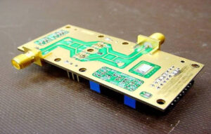
Quick-turn high frequency PCB prototyping is the process of rapidly fabricating RF or microwave circuit board samples while still controlling material selection, impedance, stackup, signal loss, and manufacturing tolerances. Unlike standard PCB prototypes, high-frequency PCB prototypes are more sensitive to material availability, dielectric thickness, copper roughness, controlled impedance, lamination process, surface finish, and DFM review.
For R&D teams, speed matters. A delayed prototype can slow down RF testing, antenna tuning, product validation, and customer demos. However, rushing a high-frequency PCB prototype without proper manufacturing review can create a different problem: the board may arrive quickly but fail to match the expected RF performance.
That is why quick-turn RF PCB prototyping must balance lead time and quality. The goal is not only to build the board fast, but also to make sure the prototype can support meaningful testing.
Mars-PCB supports customers working on high-frequency PCB fabrication for RF, microwave, communication, radar, and other high-frequency applications. For prototype projects, clear technical files and early DFM communication can help reduce delays and avoid avoidable manufacturing risks.
What Is High-Frequency PCB Prototyping?
High-frequency PCB prototyping refers to the small-batch or sample fabrication of printed circuit boards designed for RF, microwave, wireless, radar, antenna, satellite communication, and other high-frequency circuits.
These prototypes are often used to:
- Verify RF circuit performance
- Test impedance behavior
- Evaluate insertion loss
- Validate antenna or RF module design
- Confirm material selection
- Check mechanical fit
- Support customer samples
- Prepare for pilot production
- Identify DFM issues before volume manufacturing
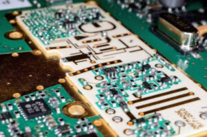
A high-frequency PCB prototype is not just a visual or mechanical sample. In many applications, it is part of the electrical system. The substrate, stackup, trace width, via structure, copper profile, and surface finish can all affect test results.
A useful high-frequency PCB prototype should be fast enough to support development schedules, but controlled enough to represent the final product’s electrical behavior.
Why Quick-Turn RF PCB Prototyping Is More Difficult Than Standard PCB Prototyping
Standard PCB prototypes are often driven by board outline, layer count, copper thickness, solder mask, surface finish, and basic electrical connectivity. High-frequency PCB prototypes require these factors plus additional RF-related controls.
The main differences include:
| Item | Standard PCB Prototype | High-Frequency PCB Prototype |
| Main goal | Verify circuit connection and mechanical layout | Verify RF/microwave signal behavior and manufacturability |
| Common material | FR4 or standard laminate | Low-loss materials, PTFE-based laminates, Rogers-type materials, ceramic-filled laminates, or high-frequency FR4 variants |
| Key concern | Open/short test, solderability, dimensions | Dk, Df, impedance, insertion loss, copper roughness, stackup stability |
| Stackup requirement | Often flexible in early prototypes | Should be clearly defined for RF performance |
| Lead time sensitivity | Mainly affected by layer count and process | Also affected by material availability, impedance review, lamination, and testing |
| DFM importance | Useful | Critical for avoiding RF performance and fabrication issues |
| Risk if rushed | Assembly or connectivity issues | Connectivity may pass, but RF performance may fail |
In other words, quick-turn high-frequency PCB prototyping requires both speed and engineering discipline.
What Affects High-Frequency PCB Prototype Lead Time?
Prototype lead time is not determined by board size alone. For high-frequency circuit boards, several technical and supply-chain factors can influence how quickly a board can be manufactured.
1. Material Availability
Material availability is one of the biggest factors affecting high-frequency PCB prototype lead time. Standard FR4 is widely available, but RF and microwave materials may have different procurement cycles.
Materials that may affect lead time include:
- Rogers-type high-frequency laminates
- PTFE-based materials
- Ceramic-filled PTFE laminates
- Taconic-type RF materials
- Low-loss FR4 variants
- Low-loss prepregs
- Hybrid stackup materials
If the exact material is not in stock, the project may need more time for procurement. If the design allows an approved alternative material, the prototype may move faster.
For quick-turn RF PCB prototyping, material confirmation should happen before the final quotation, not after the order is placed.
2. Layer Count and Stackup Complexity
A simple two-layer RF board is usually easier to prototype than a multilayer high-frequency PCB with controlled impedance, buried structures, hybrid materials, or special lamination requirements.
Lead time may increase when the design includes:
- Multilayer RF stackups
- Hybrid material combinations
- Multiple impedance structures
- Tight dielectric thickness requirements
- Blind or buried vias
- Sequential lamination
- Special bonding materials
- Thick copper or mixed copper weights
For high-frequency prototypes, the stackup should not be treated as a flexible manufacturing detail. It is part of the RF design.
3. Controlled Impedance Requirements
Controlled impedance is common in RF PCB prototyping. However, impedance control requires stackup review, trace width verification, dielectric thickness confirmation, and process planning.
A controlled impedance prototype may take more review time if:
- Impedance values are missing
- Trace layers are not clearly identified
- Dielectric thickness is not defined
- Material Dk is uncertain
- Trace width is too narrow for the required impedance
- Copper thickness after plating is not considered
- Different impedance values exist on multiple layers
A manufacturer can usually review these issues more efficiently when the customer provides a complete impedance table.
4. DFM Review Time
DFM review is sometimes seen as a delay, but for high-frequency PCB prototyping it often saves time by preventing production problems.
A DFM review may check:
- Minimum trace width and spacing
- Drill size and annular ring
- Layer registration risk
- Copper-to-edge clearance
- Solder mask clearance
- RF trace geometry
- Via structure
- Stackup feasibility
- Material compatibility
- Impedance feasibility
- Surface finish compatibility
Skipping DFM review may shorten the front-end process, but it can increase the risk of fabrication delays, redesign, or unusable RF test results.
5. Surface Finish Selection
Surface finish affects solderability, assembly reliability, storage conditions, and in some cases RF performance. Common options include ENIG, immersion silver, OSP, immersion tin, and other finishes depending on application needs.
Surface finish can affect lead time if:
- The chosen finish is not part of the standard quick-turn process
- The board requires special assembly compatibility
- The application has wire bonding or RF launch requirements
- The finish needs additional process control
- The finish is not available for the selected material or board structure
For RF prototypes, surface finish should be selected based on both assembly and electrical requirements.
6. Hole Structure and Via Requirements
Vias are important in high-frequency circuits because they can introduce discontinuities, stubs, parasitic effects, and return-path issues. A simple through-hole via structure is usually faster than blind vias, buried vias, back-drilled vias, or complex HDI structures.
Lead time may increase if the prototype requires:
- Blind vias
- Buried vias
- Laser vias
- Back drilling
- Filled and capped vias
- Via-in-pad
- Tight via registration
- Heavy plating control
In many RF prototypes, designers try to minimize unnecessary signal layer transitions. This can improve both performance and manufacturability.
7. Testing and Inspection Requirements
Every PCB prototype should pass basic manufacturing checks, but high-frequency prototypes may require additional verification depending on project requirements.
Possible checks include:
| Testing or Inspection Item | Purpose |
| Electrical open/short test | Confirms basic connectivity |
| Dimensional inspection | Checks outline, trace width, hole size, and spacing |
| Impedance testing | Confirms controlled impedance structures |
| Cross-section analysis | Reviews plating, dielectric thickness, and layer structure |
| Visual inspection | Checks surface defects and solder mask quality |
| Material verification | Confirms material type and stackup details |
| Customer RF testing | Often performed after assembly or system integration |
More testing may increase lead time, but it can also reduce risk for critical RF prototypes.
What Affects High-Frequency PCB Prototype Quality?
Fast delivery is only valuable if the prototype can support useful engineering validation. Quality in high-frequency PCB prototyping is affected by material control, stackup accuracy, trace geometry, copper profile, lamination, and process consistency.
Material Consistency
The chosen material should match the design assumptions. If the actual material has a different Dk, Df, thickness, or copper profile, the prototype may not behave as expected.
A good RF prototype process should confirm:
- Material type
- Dielectric thickness
- Copper weight
- Copper profile, if specified
- Prepreg or bonding material
- Approved substitutes, if any
Impedance Accuracy
Impedance accuracy depends on trace width, dielectric thickness, Dk, copper thickness, and etching tolerance. For RF and microwave prototypes, impedance mismatch can create reflection, loss, tuning difficulty, or measurement variation.
Important quality factors include:
- Accurate stackup
- Controlled etching
- Correct copper thickness
- Consistent dielectric thickness
- Clear impedance requirements
- Proper reference plane structure
Copper Roughness and Conductor Loss
At high frequencies, current tends to flow near the copper surface. Copper roughness can therefore affect conductor loss. For low-loss RF paths, smoother copper may be preferred in many applications, but the copper type must still be compatible with fabrication and reliability requirements.
Lamination Stability
High-frequency materials may behave differently during lamination compared with standard FR4. Lamination quality affects dielectric thickness, bonding, warpage, and impedance consistency.
Quality risks may include:
- Dielectric thickness variation
- Voids
- Poor bonding
- Warpage
- Layer shift
- Inconsistent impedance
RF Trace Geometry
Trace geometry is directly connected to RF performance. Even when a board passes open/short testing, small trace width changes may affect impedance and transmission behavior.
For high-frequency prototypes, engineers should pay attention to:
- Trace width
- Trace spacing
- Coupling gap
- Pad transitions
- RF launch areas
- Antenna feed structures
- Via transition geometry
- Ground clearance
- Reference plane continuity
Lead Time vs Quality: What Can Be Accelerated and What Should Not Be Rushed?
Quick-turn prototyping does not mean every step should be compressed equally. Some steps can be accelerated through preparation, while others should remain carefully controlled.
| Process Area | Can Be Accelerated? | Notes |
| Quotation | Yes | Complete files and clear requirements help speed up review |
| Material confirmation | Sometimes | Faster if materials are in stock or approved alternatives are allowed |
| DFM review | Partly | Can be efficient, but should not be skipped for RF boards |
| Stackup confirmation | Yes, with preparation | Provide stackup and impedance details early |
| Lamination | Limited | Must follow material and process requirements |
| Drilling and plating | Limited | Quality control should not be rushed |
| Surface finish | Depends | Standard finishes may be faster than special options |
| Testing | Limited | Critical checks should not be removed only to save time |
| Customer approval | Yes | Fast responses to engineering questions can reduce delays |
The fastest high-frequency PCB prototype projects usually start with complete files, confirmed materials, clear impedance requirements, and quick engineering communication.
What Files Are Needed for Quick-Turn High-Frequency PCB Prototyping?
Incomplete technical information is one of the most common causes of prototype delays. For quick-turn RF PCB fabrication, customers should prepare a complete data package.
| File or Information | Why It Matters |
| Gerber files | Defines copper layers, solder mask, silkscreen, and board geometry |
| Drill files | Defines hole sizes, locations, and drill types |
| Stackup drawing | Defines layer order, dielectric thickness, copper thickness, and material |
| Material specification | Helps confirm RF performance and availability |
| Controlled impedance table | Supports impedance calculation and fabrication planning |
| Board thickness | Affects mechanical and electrical behavior |
| Copper weight | Affects impedance, loss, current capacity, and etching |
| Surface finish | Affects assembly, solderability, and reliability |
| Quantity | Affects production planning and cost |
| Special requirements | Includes RF notes, via plugging, tolerance, testing, and packaging |
| Assembly information, if needed | Helps coordinate prototype PCB and assembly requirements |
For urgent projects, customers should avoid sending only Gerber files with no stackup or material notes. A complete package helps the manufacturer quote faster and identify risks earlier.
Common Reasons High-Frequency PCB Prototypes Are Delayed
1. Material Is Not Clearly Specified
If the customer only writes “high-frequency material” or “Rogers equivalent,” the manufacturer may need additional confirmation. This can slow down quotation and production.
2. Stackup Is Missing or Incomplete
High-frequency PCB performance depends on stackup. Missing dielectric thickness or copper thickness can delay impedance review.
3. Impedance Requirements Are Unclear
If controlled impedance traces are not identified, the manufacturer may need to ask follow-up questions before production.
4. Design Rules Are Too Aggressive
Very narrow lines, tight spacing, small annular rings, or complex via structures may require additional process review.
5. Surface Finish Is Not Matched to the Application
Some surface finishes may not be suitable for the intended assembly process or RF requirements. Clarification may be needed.
6. Engineering Questions Are Not Answered Quickly
Quick-turn projects require fast communication. Delayed responses to DFM questions can extend the schedule more than the manufacturing process itself.
How to Improve Prototype Lead Time Without Sacrificing Quality
Confirm Materials Early
Before finalizing the design, check whether the required high-frequency material is available. If acceptable, define substitute materials in advance.
Provide a Complete Stackup
A clear stackup helps the manufacturer review impedance, dielectric thickness, material compatibility, and lamination feasibility.
Identify RF-Critical Areas
Mark RF traces, antenna feed lines, impedance-controlled traces, and sensitive transitions. This helps the manufacturer focus DFM review on the most important areas.
Avoid Unnecessary Complexity
Every additional process can affect lead time. Avoid blind vias, buried vias, via-in-pad, tight tolerances, or special finishes unless they are necessary.
Use Practical Tolerances
Overly tight tolerances can increase cost and lead time. Use tight tolerances only where they affect electrical or mechanical performance.
Respond Quickly to DFM Feedback
Fast engineering communication is one of the most effective ways to keep a quick-turn prototype on schedule.
Mars-PCB provides high-frequency PCB prototyping and fabrication support for customers who need engineering review before prototype production.
Quick-Turn High-Frequency PCB Prototype Checklist
Use this checklist before submitting a quick-turn RF PCB prototype order.
| Checklist Item | Confirmed? |
| Gerber files are complete | Yes / No |
| Drill files are included | Yes / No |
| Stackup drawing is provided | Yes / No |
| Material type is clearly specified | Yes / No |
| Approved material alternatives are listed | Yes / No |
| Controlled impedance values are defined | Yes / No |
| RF-critical traces are identified | Yes / No |
| Copper weight is specified | Yes / No |
| Board thickness is specified | Yes / No |
| Surface finish is selected | Yes / No |
| Special tolerances are clearly marked | Yes / No |
| Testing requirements are defined | Yes / No |
| Quantity and delivery expectations are provided | Yes / No |
| Contact person can respond to DFM questions quickly | Yes / No |
This kind of checklist helps both the buyer and manufacturer avoid unnecessary back-and-forth communication.
How to Choose a Quick-Turn High-Frequency PCB Prototype Manufacturer
A reliable high-frequency PCB prototype manufacturer should be able to support both speed and technical review. The supplier should understand RF material selection, stackup control, controlled impedance, lamination risk, copper roughness, and prototype quality requirements.
When choosing a supplier, evaluate:
| Supplier Capability | Why It Matters |
| High-frequency material experience | Helps reduce risk with RF and microwave laminates |
| Material availability support | Affects prototype lead time directly |
| Stackup review capability | Supports predictable impedance and RF behavior |
| Controlled impedance process | Important for RF transmission lines |
| DFM feedback | Helps prevent fabrication delays and design issues |
| Prototype production flexibility | Supports urgent R&D schedules |
| Communication speed | Reduces delays during engineering review |
| Quality inspection process | Helps ensure prototypes are useful for testing |
| Transition to production | Helps move from prototype to pilot or volume build |
A quick-turn supplier should not simply say “yes” to every urgent request. For RF and microwave prototypes, a responsible manufacturer should review whether the requested delivery time is compatible with the required material, stackup, process, and quality checks.
For projects involving RF circuits, microwave boards, radar modules, antennas, or communication equipment, Mars-PCB can support custom high-frequency PCB prototype fabrication with manufacturing-focused communication.
FAQ: Quick-Turn High-Frequency PCB Prototyping
1. What is high frequency PCB prototyping?
High frequency PCB prototyping is the sample fabrication of RF or microwave circuit boards used to validate material selection, stackup, controlled impedance, signal loss, assembly fit, and circuit performance before pilot or mass production.
2. What affects quick-turn RF PCB lead time?
Quick-turn RF PCB lead time is affected by material availability, layer count, stackup complexity, controlled impedance requirements, surface finish, via structure, DFM review, testing requirements, and customer response speed during engineering questions.
3. Can high-frequency PCB prototypes be made with FR4?
Some high-frequency PCB prototypes can use low-loss FR4 or specialized FR4 variants, depending on frequency and performance requirements. For demanding RF or microwave circuits, low-loss materials such as PTFE-based or Rogers-type laminates are often preferred.
4. Why is DFM review important for high-frequency PCB prototypes?
DFM review is important because high-frequency PCB prototypes are sensitive to material choice, impedance, trace geometry, dielectric thickness, vias, and lamination. DFM review helps identify risks before fabrication begins.
5. What files are required for high frequency PCB prototype fabrication?
Commonly required files include Gerber files, drill files, stackup drawing, material specification, controlled impedance table, copper weight, board thickness, surface finish, quantity, and any special RF or microwave design notes.
6. Does controlled impedance increase PCB prototype lead time?
Controlled impedance can add review time because the manufacturer needs to confirm stackup, material Dk, dielectric thickness, copper thickness, and trace geometry. However, clear impedance requirements can help avoid delays and improve prototype reliability.
7. How can I reduce high-frequency PCB prototype delays?
You can reduce delays by confirming material availability early, providing complete fabrication files, defining impedance requirements, choosing practical tolerances, avoiding unnecessary process complexity, and responding quickly to DFM questions.
Conclusion
Quick-turn high-frequency PCB prototyping is not only about making RF or microwave boards faster. It is about building prototypes quickly while maintaining the material, stackup, impedance, copper, lamination, and inspection controls needed for meaningful RF testing.
Lead time is affected by material availability, layer count, controlled impedance, surface finish, via structure, testing requirements, and DFM communication. Quality is affected by material consistency, dielectric thickness, trace geometry, copper roughness, impedance control, and lamination stability.
For R&D teams, the best way to speed up high-frequency PCB prototype fabrication is to prepare complete technical files and communicate with the manufacturer early. If your project involves RF modules, microwave circuits, antennas, radar systems, or communication equipment, Mars-PCB can support your development with high-frequency PCB prototyping and fabrication services.