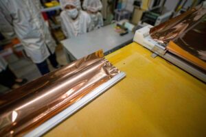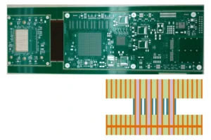
An RF PCB for radar systems must support stable high-frequency signal transmission, low insertion loss, controlled impedance, accurate antenna geometry, and reliable thermal performance. Unlike general-purpose PCBs, radar PCBs are part of the RF signal path, so material selection and fabrication tolerance directly affect detection range, resolution, sensitivity, and repeatability.
Radar circuits often work with microwave or millimeter-wave signals. In automotive radar, 77/79 GHz systems are widely used for ADAS and automated driving functions, which makes PCB material and fabrication quality especially important for antenna arrays, RF front-end circuits, and high-frequency interconnects.
For engineers and purchasing teams, the core question is not simply “Can this supplier make a radar PCB?” A better question is: can the supplier manufacture the required RF PCB stackup with the right material, impedance control, copper quality, via structure, and tolerance for the radar system?
Mars-PCB provides RF PCB for radar systems and other high-frequency PCB fabrication support for projects requiring low-loss materials, controlled impedance, and RF-focused manufacturability review.
Radar PCBs Are Performance-Critical, Not Just Frequency-Critical
A radar PCB does more than connect components. It helps shape, transmit, receive, and preserve RF signals. In many radar modules, the PCB may include RF transmission lines, antenna arrays, power amplifier connections, low-noise amplifier paths, filters, mixers, oscillators, and high-speed control or signal-processing interfaces.
The PCB design and fabrication quality can influence:
| Radar Performance Area | PCB-Related Influence |
| Detection sensitivity | Signal loss, noise coupling, RF trace quality |
| Range performance | Insertion loss, antenna efficiency, RF front-end stability |
| Angular resolution | Antenna geometry accuracy and phase consistency |
| Frequency stability | Material Dk stability and stackup control |
| Signal repeatability | Impedance control and fabrication tolerance |
| Thermal reliability | Material CTE, copper distribution, heat dissipation |
| EMI behavior | Grounding, shielding, via fences, return path control |
For radar systems, PCB variation can become RF performance variation. A slight shift in trace width, dielectric thickness, copper roughness, or antenna geometry may not look serious mechanically, but it can affect impedance, phase, radiation pattern, or signal loss.
Common Radar PCB Applications
Radar PCB requirements vary depending on application. An industrial motion sensor, a 24 GHz radar module, and a 77 GHz automotive radar board may all be called radar PCBs, but their material and manufacturing priorities are not identical.
| Radar Application | Typical PCB Priority |
| Automotive radar | Low loss, antenna accuracy, thermal stability, high repeatability |
| Industrial radar sensors | Reliability, cost-performance balance, stable RF behavior |
| Security and perimeter radar | Signal sensitivity, environmental durability |
| Aerospace and defense radar | High reliability, tight process control, advanced RF materials |
| Smart traffic radar | Long-term stability and outdoor reliability |
| Level measurement radar | Material stability and controlled RF transmission |
| Short-range radar modules | Compact layout and RF/digital isolation |
Automotive radar is especially demanding because radar modules must fit compact spaces, support high-frequency operation, and maintain stable performance under temperature and vibration conditions. Infineon describes 77/79 GHz radar as relevant to automotive safety-critical applications such as automatic emergency braking and automated driving functions.
Material Selection for Radar RF PCBs
Material is one of the first decisions in radar PCB fabrication. Standard FR-4 may be acceptable for some lower-frequency or non-critical control sections, but many radar RF sections require low-loss, high-frequency materials.
Important material properties include:
| Material Property | Why It Matters for Radar PCBs |
| Dk / dielectric constant | Affects impedance, wavelength, antenna size, and phase behavior |
| Df / dissipation factor | Affects dielectric loss and insertion loss |
| Dk tolerance | Influences repeatability between boards |
| Thickness tolerance | Affects impedance and antenna performance |
| Copper roughness | Affects conductor loss at microwave/mmWave frequencies |
| CTE | Affects reliability during thermal cycling |
| Moisture absorption | Can influence long-term electrical stability |
| Thermal conductivity | Important near RF power devices |
| Lamination compatibility | Critical for multilayer and hybrid radar stackups |
Radar PCB material should be chosen by frequency, loss budget, antenna structure, thermal environment, and manufacturability—not only by brand name.
Common material categories for radar PCB fabrication include Rogers materials, PTFE-based laminates, ceramic-filled PTFE composites, Taconic materials, Isola low-loss materials, and selected high-frequency FR-4 alternatives. Rogers describes its RO4000 laminates as materials used in microwave and millimeter-wave frequency designs, while Mars-PCB also lists Rogers, Taconic, PTFE/Teflon-based materials, ceramic-filled PTFE composites, and low-loss prepregs for high-frequency applications.
Rogers, PTFE, and Hybrid Materials in Radar PCBs
Radar projects often use low-loss laminates because radar signals can be sensitive to dielectric and conductor losses. However, material selection is not a one-size-fits-all decision.
Rogers Materials
Rogers materials are commonly used in RF, microwave, and millimeter-wave PCB applications. Some Rogers material families are designed for lower-loss performance, stable Dk, and high-frequency use. Rogers RO4000 series materials, for example, are positioned for microwave and millimeter-wave frequency designs.
Rogers-type materials may be considered when the design requires:
- Controlled impedance RF transmission lines
- Radar antenna arrays
- Microwave or millimeter-wave circuits
- Lower loss than standard FR-4
- Stable high-frequency behavior
- Hybrid RF/digital stackups
PTFE-Based Materials
PTFE-based materials are often selected for low-loss RF and microwave circuits. They can be suitable for high-frequency radar sections, but they may require more careful fabrication control than standard epoxy-glass materials.
PTFE-based radar PCB considerations include:
- Drilling and hole wall preparation
- Lamination control
- Dimensional stability
- Copper adhesion
- Material handling
- Cost and lead time
Hybrid Stackups
Many radar PCBs are not purely RF boards. They may combine an RF antenna/front-end region with digital control, power management, MCU, connector, or signal-processing sections. In such cases, a hybrid stackup may combine RF laminate layers with FR-4 or other PCB materials.
Hybrid stackups can help balance performance and cost, but they require careful review of:
- Material CTE mismatch
- Lamination compatibility
- Dielectric thickness
- Impedance transition
- Via reliability
- Warpage risk
- Production repeatability
Stackup Design: Where Radar PCB Performance Is Built
Radar PCB stackup design controls how RF energy travels through the board. The stackup defines the relationship between RF traces, dielectric materials, ground planes, antenna structures, and power or digital layers.
A radar PCB stackup should clarify:
- RF signal layer
- Antenna layer if integrated on PCB
- Reference ground plane
- Dielectric material and thickness
- Copper thickness
- Transmission line type
- Controlled impedance target
- Ground via strategy
- Shielding and isolation regions
- Digital and power layer separation
A radar PCB stackup should be reviewed before layout is finalized, because dielectric thickness and material choice determine RF trace geometry and antenna dimensions.
For example, if the RF designer expects a certain dielectric thickness but the manufacturer uses a different available core or prepreg, the impedance and antenna tuning may shift. This may require layout changes rather than a simple manufacturing note correction.
Mars-PCB can support radar PCB material and stackup review before fabrication to help engineering teams check whether the design is practical for production.
Transmission Line Structures in Radar PCBs
Radar PCB layouts may use different RF transmission line structures depending on frequency, layout density, shielding needs, and antenna architecture.
| Structure | Where It May Be Used | Key Fabrication Concern |
| Microstrip | Surface RF routing, antenna feed lines, accessible RF paths | Dielectric thickness, solder mask, copper roughness |
| Stripline | Shielded RF routing inside multilayer boards | Layer registration and dielectric symmetry |
| Grounded coplanar waveguide | Compact RF routing and mmWave layouts | Trace width, ground gap, via fence, plating control |
| Coplanar waveguide | Specialized RF layouts | Gap precision and ground control |
| PCB antenna array | Integrated radar antennas | Etching accuracy, Dk stability, copper profile |
For radar antennas, conductor geometry is especially sensitive. Antenna patch size, feed line length, spacing, and copper accuracy may affect the radiation pattern and phase response. At mmWave frequencies, even small mechanical tolerances become more important than in lower-frequency PCB designs.
Controlled Impedance and Phase Consistency
Controlled impedance is essential for radar PCB fabrication. Many RF lines are designed around 50-ohm impedance, although actual system requirements may vary.
Radar PCB impedance is influenced by:
- Trace width
- Trace spacing
- Dielectric thickness
- Dk value
- Copper thickness
- Copper roughness
- Solder mask
- Ground plane distance
- Etching tolerance
- Plating variation
For radar arrays, phase consistency may be as important as impedance. If multiple antenna feed paths are intended to have matched phase behavior, differences in line length, dielectric thickness, or etching quality can degrade consistency.
In radar PCB fabrication, controlled impedance and phase repeatability depend on both design calculation and manufacturing process control.
Engineers should provide an impedance table, stackup drawing, RF line requirements, and antenna area notes before fabrication.
Copper Roughness and Signal Loss
At high frequencies, current concentrates near the surface of the conductor. This skin effect makes copper roughness more important in radar PCB fabrication. Rougher copper can increase conductor loss, especially for microwave and millimeter-wave signals.
This does not mean every radar PCB must use the smoothest copper option. The right choice depends on the frequency, path length, antenna design, loss budget, and cost target. However, copper roughness should not be ignored when the board operates in high-frequency radar bands.
Engineers should ask the PCB supplier:
- What copper foil type is used?
- Is low-profile copper available for the selected material?
- Is finished copper thickness included in impedance calculation?
- How is etching compensation handled?
- Can the supplier maintain trace width tolerance for antenna features?
Thermal Stability in Radar PCB Fabrication
Radar boards may include RF power amplifiers, transceivers, processors, voltage regulators, and other heat-generating devices. Thermal behavior matters because temperature variation can influence material properties, solder joint reliability, and RF performance.
Thermal design considerations include:
| Thermal Factor | PCB Design Impact |
| Material CTE | Affects expansion and mechanical stress |
| Tg and thermal stability | Affects reliability during assembly and operation |
| Copper distribution | Helps spread heat but may affect RF fields |
| Thermal vias | Improve heat transfer but must avoid RF disturbance |
| Component placement | Separates heat sources from sensitive RF areas |
| Stackup symmetry | Helps reduce warpage risk |
For automotive radar, thermal stability is particularly important because the module may operate in harsh environments. For industrial or outdoor radar systems, humidity, temperature cycling, and long operating hours may also affect material and finish selection.
Fabrication Tolerances That Matter in Radar PCBs
Radar PCB fabrication requires closer attention to tolerance than many general PCB projects. The following tolerances should be discussed before production.
| Fabrication Factor | Radar PCB Risk If Poorly Controlled |
| Trace width tolerance | Impedance shift and antenna variation |
| Dielectric thickness tolerance | Phase and impedance inconsistency |
| Layer registration | Misalignment in multilayer RF structures |
| Drill accuracy | Poor via transitions and grounding |
| Copper plating | Finished copper variation and impedance shift |
| Etching quality | Feed line and antenna geometry errors |
| Solder mask alignment | RF trace or antenna interference |
| Board flatness | Assembly and RF module integration issues |
Radar PCB fabrication should be evaluated by electrical risk, not only by whether the board meets basic mechanical drawing requirements.
Radar PCB Design Review Before Fabrication
Before sending radar PCB files to production, engineers should prepare a complete review package. This improves quotation accuracy and reduces engineering back-and-forth.
| File or Requirement | Why It Matters |
| Gerber or ODB++ files | Defines copper, solder mask, silkscreen, and outline |
| Drill files | Defines plated and non-plated holes |
| Stackup drawing | Confirms material, dielectric thickness, copper, and layers |
| Material specification | Prevents unsuitable substitution |
| Impedance table | Defines target impedance and tolerance |
| RF critical area notes | Highlights antenna, feed line, and RF transition zones |
| Surface finish requirement | Affects assembly and RF/contact behavior |
| Solder mask notes | Important for antenna and RF trace exposure |
| Via requirements | Defines grounding, via fences, and RF transitions |
| Quantity and phase | Helps plan prototype, pilot run, or production |
For radar projects moving toward prototype or production, engineers can share these files with Mars-PCB high-frequency PCB fabrication for DFM and manufacturing feasibility review.
Common Mistakes in Radar PCB Projects
Mistake 1: Selecting a Material Without Checking Fabrication Capability
A material may look suitable on a datasheet but still create fabrication challenges. Always confirm whether the PCB supplier can process the selected laminate, thickness, copper type, and stackup.
Mistake 2: Treating Antenna Geometry Like Normal Copper Routing
Radar antenna features require precision. Small deviations in patch size, spacing, or feed structure may affect performance. Antenna copper should be marked as RF-critical during fabrication review.
Mistake 3: Ignoring the Ground Return Path
Radar RF traces need stable reference planes and short return paths. Split ground planes, poor stitching, or gaps under RF traces can create discontinuities and radiation issues.
Mistake 4: Overlooking Via Fence Design
Via fences are often used to improve isolation and field control. Poor via spacing or inconsistent grounding can reduce the intended shielding effect.
Mistake 5: Separating Electrical Design from Manufacturing Review
Radar PCB performance depends on the interaction between simulation, layout, material, and fabrication. If the manufacturer is involved only after Gerbers are finished, critical stackup or tolerance issues may be discovered late.
How to Choose an RF PCB Supplier for Radar Systems
A radar PCB supplier should understand high-frequency materials, controlled impedance, RF stackup design, fine copper feature control, via reliability, and DFM review.
Before placing an order, ask:
- Can you process the specified RF or microwave laminate?
- Can you support the required dielectric thickness and copper type?
- Can you review impedance based on the actual manufacturable stackup?
- Can you control antenna copper features and trace tolerance?
- Can you support grounded coplanar waveguide or microstrip structures?
- Can you provide impedance testing if required?
- Can you handle hybrid radar PCB stackups?
- What surface finish do you recommend for this radar application?
- What DFM risks do you see in the antenna or RF feed area?
- Can the prototype process be scaled toward production?
For broader PCB manufacturing or project support, Mars-PCB’s custom PCB manufacturing service can be reviewed alongside its RF/high-frequency PCB capabilities.
FAQ
What is an RF PCB for radar systems?
An RF PCB for radar systems is a high-frequency circuit board designed to support radar signal transmission, reception, antenna structures, RF front-end circuits, and controlled impedance paths. It requires suitable low-loss materials and precise fabrication control.
What material is used for radar PCB fabrication?
Common radar PCB materials include Rogers laminates, PTFE-based materials, ceramic-filled PTFE composites, Taconic materials, Isola low-loss laminates, and selected high-frequency FR-4 alternatives. The right material depends on frequency, loss budget, stackup, and cost target.
Why is low-loss material important for radar PCBs?
Low-loss material helps reduce dielectric loss and preserve RF signal energy. This is important for radar systems because signal loss can affect sensitivity, range, antenna performance, and overall RF front-end efficiency.
Is automotive radar PCB different from general RF PCB?
Yes. Automotive radar PCBs often require higher frequency performance, compact antenna structures, thermal stability, controlled impedance, and repeatable fabrication. Many automotive radar systems operate around 77/79 GHz, making material and tolerance control especially important.
What should engineers provide before radar PCB fabrication?
Engineers should provide Gerber or ODB++ files, drill files, stackup drawing, material specification, impedance table, RF critical area notes, solder mask requirements, via requirements, surface finish, and prototype or production quantity.
Can FR-4 be used for radar PCB design?
FR-4 may be used in some lower-frequency or non-critical control sections, but many radar RF sections require lower-loss high-frequency materials. The decision should be based on frequency, insertion loss, impedance stability, and reliability requirements.
How do I choose a radar PCB manufacturer?
Choose a radar PCB manufacturer that can review RF materials, controlled impedance, stackup design, antenna copper features, via structures, copper roughness, and DFM risks before fabrication. The supplier should understand both PCB manufacturing and RF performance requirements.
Conclusion
RF PCBs for radar systems require more than ordinary PCB fabrication. Material selection, dielectric thickness, copper roughness, controlled impedance, antenna geometry, via fences, ground planes, surface finish, and thermal behavior all influence radar performance.
For engineering teams, the safest approach is to involve the PCB manufacturer before finalizing the design. Confirm the RF material, stackup, impedance targets, antenna-critical areas, and fabrication tolerance early. This can reduce the risk of signal loss, antenna shift, prototype failure, and production inconsistency.
Mars-PCB supports RF PCB for radar systems with high-frequency PCB fabrication, material review, controlled impedance support, and DFM feedback for radar-related applications.