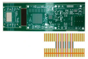
An RF PCB stackup defines the layer structure, dielectric thickness, copper weight, reference planes, and transmission line geometry that control impedance, signal loss, crosstalk, and electromagnetic behavior. For high-frequency performance, engineers must plan the stackup before fabrication instead of treating it as a general PCB manufacturing detail.
In RF PCB design, the board is not only a carrier for components. It becomes part of the electrical circuit. Microstrip lines, stripline structures, ground planes, dielectric materials, via transitions, and solder mask conditions all influence how RF signals propagate.
A reliable RF PCB stackup should answer several questions before production: Which layer carries RF signals? Where is the reference ground plane? What dielectric material and thickness are used? What impedance must be controlled? Will the design use microstrip, stripline, grounded coplanar waveguide, or a hybrid structure? Can the selected PCB manufacturer fabricate the stackup consistently?
Mars-PCB provides RF PCB stackup support for high-frequency PCB and RF circuit board projects, helping engineers review materials, impedance requirements, and manufacturability before fabrication.
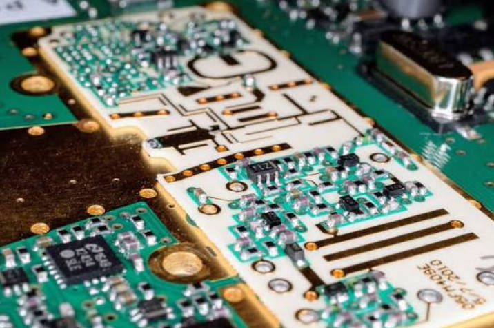
What Is an RF PCB Stackup?
An RF PCB stackup is the planned arrangement of copper layers, dielectric layers, ground planes, power planes, and signal layers in a high-frequency printed circuit board. It defines how RF signals are routed and how electromagnetic fields are controlled.
A stackup usually includes:
- Signal layers
- Ground reference planes
- Power planes
- RF dielectric materials
- Core and prepreg thicknesses
- Copper thickness
- Controlled impedance structures
- Via strategy
- Solder mask and surface finish requirements
For standard digital PCBs, the stackup is often optimized for routing density, cost, power distribution, and mechanical requirements. For RF PCBs, the stackup directly affects impedance, insertion loss, phase stability, return loss, isolation, and radiation.
In high-frequency PCB stackup design, every physical layer decision can become an electrical performance decision.
Why RF PCB Stackup Design Matters
At low frequencies, PCB traces can often be treated as simple conductors. At RF and microwave frequencies, traces behave as transmission lines. This means that their geometry and surrounding dielectric environment determine characteristic impedance and signal behavior.
If the stackup is poorly designed, the PCB may suffer from:
- Impedance mismatch
- Higher insertion loss
- Poor return loss
- Unstable antenna tuning
- Increased radiation
- Crosstalk between RF and digital sections
- EMI problems
- Phase variation
- Prototype-to-production inconsistency
For example, if a 50-ohm RF trace is designed on a dielectric thickness that the manufacturer cannot produce, the final board may require a different trace width. If that change happens after layout completion, routing may become difficult or the board may no longer match the intended RF performance.
RF PCB stackup design should be confirmed before layout finalization, not after Gerber files are already released.
Core Elements of an RF PCB Stackup
1. RF Material Selection
RF stackup design begins with material selection. The dielectric constant, dissipation factor, thickness tolerance, copper type, and thermal behavior of the material influence signal propagation.
Common high-frequency PCB materials include Rogers laminates, Taconic materials, Isola low-loss materials, PTFE-based laminates, ceramic-filled PTFE composites, and selected low-loss FR-4 alternatives.
Key material factors include:
| Material Factor | Why It Matters in RF Stackup Design |
| Dk / dielectric constant | Affects impedance, trace width, wavelength, and phase response |
| Df / dissipation factor | Affects dielectric loss and insertion loss |
| Thickness tolerance | Affects impedance consistency |
| Copper roughness | Affects conductor loss, especially at higher frequencies |
| CTE | Affects reliability during thermal cycling and assembly |
| Moisture absorption | May influence electrical stability |
| Thermal conductivity | Important for RF power circuits |
| Lamination compatibility | Important for multilayer and hybrid stackups |
The material should be selected based on the actual operating frequency, loss requirement, stackup structure, and production quantity. A lower-loss material may be necessary for microwave circuits, while some lower-frequency RF designs may accept a more economical material if performance targets allow it.
2. Dielectric Thickness
Dielectric thickness is one of the most important variables in RF PCB stackup design. It affects the distance between a signal trace and its reference plane, which directly influences impedance.
For a microstrip line, the trace is usually on an outer layer with a ground plane underneath. The dielectric thickness between the trace and ground plane affects the required trace width for the target impedance.
For stripline, the RF trace is embedded between two reference planes. The distance to each plane affects impedance, field containment, and loss behavior.
If the dielectric layer is too thick, the required trace width may become too wide for the layout. If it is too thin, the trace width may become very narrow and harder to fabricate consistently.
3. Copper Thickness and Copper Roughness
Copper thickness affects impedance calculation, current handling, etching behavior, and conductor loss. At high frequencies, copper roughness becomes especially important because current tends to concentrate near the conductor surface.
For RF PCB fabrication, engineers should confirm:
- Base copper thickness
- Finished copper thickness
- Plating buildup
- Copper foil type
- Copper roughness
- Etching tolerance
- Whether impedance is calculated using finished copper thickness
Copper roughness can increase conductor loss, especially in microwave and millimeter-wave designs. For many RF boards, this does not mean the smoothest copper must always be used, but copper profile should be considered when loss budget is tight.
4. Ground Plane Placement
A stable ground reference is essential for RF signal integrity. The ground plane provides the return path for RF current and helps control electromagnetic fields.
A good RF stackup usually places a solid ground plane close to the RF signal layer. This helps control impedance, reduce radiation, and improve isolation.
Poor ground plane design can cause:
- Return path discontinuity
- Unwanted radiation
- Coupling into nearby traces
- Increased EMI
- Impedance discontinuity
- Poor shielding between RF and digital circuits
A continuous ground reference under RF traces is one of the most important requirements for stable RF PCB performance.
5. Transmission Line Structure
RF PCB stackup design depends heavily on the transmission line structure. Common structures include microstrip, stripline, grounded coplanar waveguide, and coplanar waveguide.
| Structure | Basic Description | Common Use | Key Stackup Concern |
| Microstrip | Signal trace on outer layer with ground plane below | RF modules, antennas, simple RF routing | Sensitive to dielectric thickness, solder mask, nearby copper |
| Stripline | Signal trace embedded between two ground planes | Better shielding and isolation | Requires controlled inner-layer dielectric spacing |
| Grounded coplanar waveguide | Signal trace with ground beside it and ground plane below | RF, microwave, compact designs | Requires control of trace width, gap, via fence, and copper plating |
| Coplanar waveguide | Signal and ground on same layer | Specialized RF layouts | Requires precise gap and field control |
| Differential stripline/microstrip | Paired traces with controlled differential impedance | High-speed digital/RF mixed systems | Requires trace width, spacing, and plane control |
Microstrip is often easier to inspect and tune because the RF trace is on the outer layer. Stripline provides better field containment but is harder to access after fabrication. Grounded coplanar waveguide can be useful for RF and microwave designs, but it requires careful control of gap spacing, ground vias, and conductor geometry.
Microstrip vs Stripline in RF PCB Stackup
Both microstrip and stripline are common in RF PCB design, but they serve different needs.
| Factor | Microstrip | Stripline |
| Signal layer | Outer layer | Inner layer |
| Reference plane | Usually one ground plane below | Ground planes above and below |
| Field exposure | Partly exposed to air and solder mask | More contained inside dielectric |
| Fabrication visibility | Easier to inspect | Hidden after lamination |
| Shielding | Lower than stripline | Better shielding |
| Tuning access | Easier | Harder |
| Loss behavior | Depends strongly on surface condition and environment | More controlled dielectric environment |
| Common use | Antennas, RF modules, accessible RF routing | Shielded RF lines, dense multilayer designs |
For many RF designs, microstrip is used when the signal needs to connect to antennas, RF connectors, tuning components, or test points. Stripline is often used when shielding and isolation are more important.
There is no universal answer that microstrip or stripline is always better. The choice depends on frequency, layout density, isolation requirement, fabrication capability, and test strategy.
Grounded Coplanar Waveguide in RF PCB Stackups
Grounded coplanar waveguide, often abbreviated as GCPW, is frequently used in RF and microwave PCB designs. In this structure, the signal trace is on the same layer as adjacent ground copper, with a reference ground plane below. Ground vias are usually placed along the ground areas to connect them to the reference plane.
GCPW can provide strong field control and is useful in compact RF layouts. However, it is more sensitive to manufacturing variation in trace width, gap spacing, copper plating, and via placement.
A GCPW stackup should define:
- Signal trace width
- Gap between signal and ground copper
- Dielectric thickness to bottom ground plane
- Copper thickness
- Via fence pitch
- Ground clearance near components
- Solder mask condition
- Target impedance
For higher-frequency circuits, small changes in gap spacing can affect impedance. This is why engineers should not rely only on theoretical line dimensions. The structure should be reviewed with the PCB manufacturer for fabrication tolerance.
Controlled Impedance in RF PCB Stackup Design
Controlled impedance means the PCB traces are designed and manufactured to maintain a specified characteristic impedance. In RF circuits, common impedance values include 50 ohms for many RF transmission lines and 75 ohms for some video or communication applications, though the exact value depends on the system.
Impedance is affected by:
| Variable | Impact |
| Trace width | Wider traces generally reduce impedance |
| Dielectric thickness | Greater distance to ground generally increases impedance |
| Dk | Higher Dk generally reduces impedance for the same geometry |
| Copper thickness | Affects effective conductor geometry |
| Solder mask | Can affect outer-layer impedance |
| Gap to ground copper | Important in coplanar structures |
| Etching tolerance | Changes final trace width |
| Plating thickness | Can influence finished conductor dimensions |
Controlled impedance is not only a design calculation; it must be manufacturable with the selected material, copper thickness, and fabrication tolerance.
Before fabrication, engineers should provide the PCB supplier with an impedance table. The table should include layer, signal type, target impedance, tolerance, trace width, spacing, reference plane, and material information.
Example RF PCB Stackup Options
The following examples are conceptual stackup structures. They are not universal specifications. Actual stackup should be confirmed based on frequency, material, impedance, routing density, and fabrication capability.
2-Layer RF PCB Stackup
| Layer | Function |
| Top Layer | RF signal, components, microstrip routing |
| Dielectric Core | RF material or low-loss material |
| Bottom Layer | Solid ground plane |
This structure is simple and often used for antennas, RF modules, evaluation boards, and lower-complexity RF circuits. The main limitation is reduced routing flexibility and limited shielding between circuits.
4-Layer RF PCB Stackup
| Layer | Function |
| L1 | RF signal, components, microstrip or GCPW |
| L2 | Solid ground plane |
| L3 | Power or secondary ground/reference plane |
| L4 | Digital/control signals or secondary RF routing |
A 4-layer stackup is common when RF circuits need a stable ground plane while still allowing power and control routing. L2 is often used as a close reference ground for L1 RF traces.
6-Layer RF PCB Stackup
| Layer | Function |
| L1 | RF components and RF routing |
| L2 | Ground reference |
| L3 | Power or controlled signals |
| L4 | Digital/control signals |
| L5 | Ground or power reference |
| L6 | Secondary signals or shielding |
A 6-layer stackup may be used for more complex RF modules, mixed-signal boards, communication devices, or designs requiring stronger isolation.
RF PCB Stackup Design Checklist Before Fabrication
Before sending files to fabrication, engineers should prepare a clear stackup package.
| Checklist Item | What to Confirm |
| Operating frequency | Frequency range and bandwidth |
| RF material | Laminate type, Dk, Df, thickness |
| Layer arrangement | RF layer, ground layer, power layer, digital layer |
| Transmission line type | Microstrip, stripline, GCPW, CPW, differential pair |
| Target impedance | 50 ohm, 75 ohm, 100 ohm differential, or project-specific value |
| Impedance tolerance | Commonly defined by project requirement and supplier capability |
| Copper thickness | Base and finished copper |
| Copper roughness | Especially important for high-frequency loss |
| Solder mask | Whether RF traces are covered or exposed |
| Via strategy | Ground vias, via fence, blind/buried vias, back drilling if needed |
| Surface finish | Assembly and RF performance considerations |
| Test coupon | Whether impedance test coupons are required |
| DFM review | Manufacturer review before production |
For projects requiring high-frequency stackup planning, Mars-PCB can support RF PCB fabrication and stackup review before prototype or production.
Common RF PCB Stackup Mistakes
Mistake 1: Designing RF Traces Before Confirming the Stackup
If the dielectric thickness or material changes after layout, the RF trace width may also need to change. This can create routing conflicts and delay fabrication.
Mistake 2: Using a Split Ground Plane Under RF Traces
A split plane under an RF trace interrupts the return path and may cause radiation, impedance discontinuity, and EMI issues. Critical RF traces should have a continuous reference ground.
Mistake 3: Ignoring Solder Mask Effects
Solder mask can change the effective dielectric environment around outer-layer RF traces. Some RF designs require exposed traces, while others allow mask coverage. The requirement should be stated clearly.
Mistake 4: Treating Via Fences as Decorative Copper
Via fences help connect top-layer ground areas to internal or bottom ground planes. Poor via spacing or missing ground connections can reduce shielding and affect impedance in coplanar structures.
Mistake 5: Using Generic FR-4 Assumptions
High-frequency materials may have different Dk, Df, copper roughness, drilling behavior, and lamination requirements compared with standard FR-4. Stackup rules should be based on the selected material, not generic defaults.
How to Work with a PCB Manufacturer on RF Stackup Design
A qualified RF PCB manufacturer should help verify whether the proposed stackup is manufacturable and suitable for the target impedance. The supplier does not replace RF simulation, but they can identify fabrication risks that may affect real board performance.
When discussing stackup with a manufacturer, ask:
- Can this material and thickness be fabricated consistently?
- What finished copper thickness should be used for impedance calculation?
- Can the proposed trace width and gap be etched reliably?
- Can you support the required impedance tolerance?
- Do you recommend solder mask over or away from RF traces?
- Can you provide impedance test coupons?
- Are via structures and ground via spacing manufacturable?
- Can this stackup be used for both prototype and production?
- Are there lower-cost material alternatives that still meet the requirement?
For broader PCB manufacturing support, engineers can also review Mars-PCB custom PCB solutions when planning fabrication, assembly, or project-level production requirements.
FAQ
What is RF PCB stackup design?
RF PCB stackup design is the process of defining PCB layers, dielectric materials, copper thickness, reference planes, and transmission line structures to control impedance, signal loss, crosstalk, and electromagnetic performance in high-frequency circuits.
What is the best stackup for RF PCB design?
There is no universal best RF PCB stackup. A suitable stackup depends on operating frequency, material, impedance target, routing density, isolation requirement, component placement, and fabrication capability.
Should RF traces be routed as microstrip or stripline?
Microstrip is commonly used for accessible RF routing, antennas, connectors, and tuning circuits. Stripline is useful when better shielding and isolation are required. The right choice depends on the circuit frequency, layout structure, and test requirements.
Why is a ground plane important in RF PCB stackup?
A ground plane provides a stable return path, helps control impedance, reduces radiation, improves shielding, and lowers EMI risk. RF traces should usually reference a continuous ground plane without splits or gaps underneath.
How does dielectric thickness affect RF PCB impedance?
Dielectric thickness controls the distance between the RF trace and its reference plane. In many structures, a thicker dielectric increases impedance, while a thinner dielectric reduces impedance for the same trace width.
What should I provide for controlled impedance RF PCB fabrication?
You should provide the stackup drawing, target impedance, impedance tolerance, material type, dielectric thickness, copper thickness, transmission line type, solder mask requirement, and test coupon requirement if needed.
Can Mars-PCB help review an RF PCB stackup before fabrication?
Yes. Mars-PCB can review high-frequency PCB material, layer structure, controlled impedance requirements, and manufacturability before fabrication. Engineers can submit stackup and design requirements for RF PCB DFM evaluation.
Conclusion
RF PCB stackup design is a critical part of high-frequency performance. Material selection, dielectric thickness, copper thickness, reference planes, transmission line geometry, via placement, and solder mask decisions all influence impedance, loss, crosstalk, and signal stability.
For engineers, the practical workflow is clear: define the frequency and impedance target, select a suitable RF material, build the stackup around a continuous ground reference, calculate transmission line geometry, then confirm manufacturability with the PCB supplier before fabrication.
Mars-PCB can provide RF PCB stackup support for high-frequency PCB fabrication, helping engineering teams move from design requirements to a manufacturable RF circuit board.