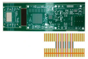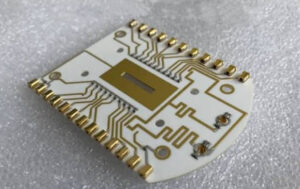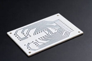
Silicon carbide and gallium nitride devices can switch faster, operate at higher power density and tolerate higher junction temperatures than conventional silicon devices. But these advantages also place more stress on the package and substrate underneath them.
That is why the choice of ceramic PCB for SiC and GaN power modules matters.
The substrate is not simply a mechanical carrier for the semiconductor. It must carry current, isolate high voltage, transfer heat, survive thermal cycling and maintain dimensional stability while the device operates at high switching speed and high power density.
For SiC and GaN power modules, substrate performance can directly influence junction temperature, current capability, module size and long-term reliability.
A wide-bandgap device may have excellent semiconductor characteristics, but those advantages can be limited if heat cannot leave the die efficiently or if the copper-to-ceramic structure cannot tolerate repeated thermal stress.
This article explains what the ceramic substrate actually does, why SiC and GaN increase the demand on the PCB structure, and how engineers can evaluate ceramic materials and copper structures for different power electronics applications.
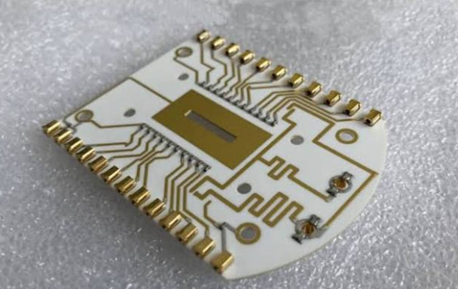
The Semiconductor Changed. The Substrate Has to Catch Up.
Traditional silicon power electronics often allow designers more room in terms of switching speed, power density and thermal loading.
SiC and GaN change that balance.
Their advantages can include:
- Higher switching frequency
- Lower switching losses in suitable designs
- Higher operating temperature capability
- Higher voltage capability for SiC
- High power density
- Smaller passive components in many converter designs
- More compact power stages
These advantages are useful only if the package around the device can support them.
A smaller, faster power stage tends to concentrate more electrical and thermal load into less area.
That creates a simple engineering problem:
The semiconductor is becoming more capable, but the thermal and mechanical path beneath it is becoming more demanding.
This is one of the main reasons ceramic substrates have become important in modern power electronics.
What Does a Ceramic PCB Actually Do in a Power Module?
A ceramic PCB performs several functions at the same time.
It is simultaneously:
- An electrical interconnection layer
- A high-voltage insulating layer
- A thermal transfer path
- A mechanical support structure
- An interface between the semiconductor and cooling system
In a power module, heat may travel through a structure similar to:
Semiconductor die → die attach → copper metallization → ceramic substrate → backside copper / interface → baseplate or heat sink
Every layer contributes thermal resistance.
If one part of this path becomes the bottleneck, the semiconductor may operate at a higher junction temperature even when the device itself is highly efficient.
The purpose of a ceramic substrate is not simply to “handle heat.” It must combine high electrical insulation with a low-resistance thermal path.
That combination is difficult to achieve with conventional organic PCB laminates at the same power density.
Why SiC Pushes the Substrate So Hard
SiC power devices are frequently used in high-voltage, high-power applications.
Typical examples include:
- EV traction inverters
- On-board chargers
- DC fast chargers
- Solar inverters
- Energy storage converters
- Industrial motor drives
- High-power DC/DC converters
These systems may use SiC MOSFETs or diodes because designers want to reduce losses while operating at high voltage and high switching frequency.
But the substrate must still deal with several demanding conditions.
High Heat Flux
Even when switching losses are reduced, the device may operate at high current and high total power.
When a large amount of heat is generated in a relatively small die area, the local heat flux becomes significant.
A substrate with insufficient thermal performance can create a large temperature gradient between the semiconductor and heat sink.
That reduces the benefit of the SiC device.
High Junction Temperature Capability
SiC devices can typically tolerate higher junction temperatures than conventional silicon power devices.
That does not mean the entire module should simply be allowed to run hotter.
Other materials may become the limiting factor:
- Solder
- Die attach
- Wire bonds
- Metallization
- Thermal interface materials
- Encapsulants
- Ceramic-to-copper interfaces
The substrate must therefore support the higher thermal environment without becoming the weakest part of the package.
Thermal Cycling
Automotive and industrial power modules rarely operate at one steady temperature.
They repeatedly:
- Power up
- Heat rapidly
- Reach load temperature
- Reduce power
- Cool down
Different materials expand by different amounts during these cycles.
Copper, ceramic and semiconductor materials all have different coefficients of thermal expansion.
Repeated mismatch generates stress.
This is especially important in high-power SiC modules because the temperature swing can be substantial.
GaN Creates a Different Substrate Challenge
GaN devices often appear in different applications than large SiC power modules.
Typical GaN applications include:
- High-frequency power supplies
- Compact AC/DC converters
- Server and data-center power systems
- Telecom power supplies
- Fast chargers
- High-frequency DC/DC converters
GaN is particularly attractive where designers want very high switching speed and small converter size.
That creates a somewhat different substrate priority.
For GaN, the substrate may need to support:
- Short current loops
- Low parasitic inductance
- Compact component placement
- Precise routing
- Fine conductor geometry
- Effective localized heat removal
SiC often pushes the substrate toward high power and thermal capacity, while GaN frequently adds stronger demands for compact geometry and low-parasitic interconnection.
There is overlap between the two, but they should not be treated as identical design problems.
SiC vs GaN: How the Substrate Priorities Differ
| Design Factor | SiC Power Module | GaN Power Module |
| Typical priority | High voltage and high power | High frequency and compact power density |
| Current level | Often high | Moderate to high depending on application |
| Heat flux | High | Can be highly localized |
| Switching frequency | High | Very high |
| Parasitic sensitivity | Important | Extremely important |
| Copper thickness | Often important | Depends on topology |
| Fine routing | Moderate to high | Often very important |
| Thermal cycling | Major concern | Application dependent |
| Typical substrate focus | Thermal path + power handling | Precision + thermal path + low parasitics |
The final substrate choice should therefore be based on the module architecture rather than simply whether the semiconductor is SiC or GaN.
Thermal Conductivity Is Only One Part of the Decision
It is tempting to compare ceramic materials using only thermal conductivity.
That is useful, but incomplete.
Common ceramic substrate materials used in power electronics may include alumina and aluminum nitride.
Typical thermal conductivity varies by material grade and manufacturing process.
In broad terms:
| Ceramic Material | Thermal Conductivity Direction | Relative Cost | Typical Design Direction |
| Alumina | Moderate | Lower | General ceramic circuits and moderate thermal loads |
| Aluminum nitride | High | Higher | High heat-flux and high-power applications |
AlN is particularly attractive for power modules because it combines electrical insulation with high thermal conductivity.
However, substrate selection must also consider:
- Thickness
- Mechanical strength
- Thermal expansion
- Board size
- Copper structure
- Cost target
- Manufacturing process
A high-conductivity ceramic does not automatically create a low thermal resistance module if the ceramic is too thick or another interface dominates the thermal path.
The complete stack-up matters.
Why AlN Often Appears in SiC Power Modules
Aluminum nitride is often considered for SiC systems because its thermal conductivity is significantly higher than commonly used alumina materials.
This can help when the design has:
- High heat flux
- Small semiconductor die area
- High module power
- Limited heat sink area
- Compact packaging
Another consideration is coefficient of thermal expansion.
AlN provides relatively favorable thermal expansion characteristics for semiconductor packaging compared with many conventional PCB materials.
This can be useful in modules subjected to repeated thermal cycling.
However, AlN is more expensive than alumina and may increase substrate and processing cost.
The correct question is therefore not:
Is AlN better?
The better question is:
Does the system need the additional thermal performance enough to justify the cost?
Copper Structure Matters Almost as Much as the Ceramic
A ceramic substrate still needs a conductive copper circuit.
For power electronics, the choice of copper formation process can strongly affect:
- Copper thickness
- Current capability
- Heat spreading
- Line width
- Spacing
- Pad dimensions
- Manufacturing precision
Two common directions are DBC and DPC.
DBC for Heavy Power Paths
DBC, or Direct Bonded Copper, is widely associated with power modules because it can support relatively thick copper structures.
That is useful when the module requires:
- High current
- Large semiconductor pads
- Strong heat spreading
- Low conductor resistance
DBC is therefore commonly evaluated for SiC power modules used in inverters, chargers and industrial power systems.
DPC for Precision and Compact Layouts
DPC, or Direct Plated Copper, forms circuitry through metallization and copper plating.
It can be advantageous where the design requires:
- Fine traces
- Small spacing
- Accurate pads
- Dense routing
- Compact interconnection
These characteristics can become useful in compact GaN-based power stages or optoelectronic and high-density ceramic circuits.
A ceramic PCB substrate design should therefore consider ceramic material and copper process as two separate but interacting decisions.
The Substrate Influences Parasitic Inductance Too
Wide-bandgap devices switch quickly.
Fast switching increases sensitivity to parasitic inductance.
Excess parasitic inductance can contribute to:
- Voltage overshoot
- Ringing
- EMI
- Switching losses
- Gate instability
The ceramic substrate itself does not solve all parasitic problems, but the circuit structure built on it affects conductor length, loop area and device placement.
This is especially important in GaN designs and increasingly important in fast-switching SiC modules.
A compact ceramic circuit can allow:
- Shorter power loops
- Closer device placement
- Optimized copper geometry
- Reduced interconnection length
For wide-bandgap power electronics, substrate layout is part of the electrical design—not only the mechanical or thermal design.
Why Copper Thickness Cannot Be Increased Without Limits
Thicker copper helps reduce electrical resistance.
That sounds ideal for high-current SiC circuits.
However, copper thickness also affects:
- Etching behavior
- Minimum line width
- Minimum spacing
- Mechanical stress
- Thermal expansion mismatch
- Manufacturing yield
This creates a design trade-off.
A power module may want very thick copper for current carrying, but a fast-switching layout may also need fine geometry.
Those requirements can conflict.
This is why the substrate process should be evaluated before the layout is completely locked.
Application Example 1: EV Traction Inverter
An EV inverter converts battery DC power into controlled AC power for the traction motor.
SiC devices are increasingly attractive in this application because of high-voltage operation and efficiency requirements.
The ceramic substrate must support:
- High current
- High voltage insulation
- Repeated thermal cycling
- Strong heat transfer
- Mechanical reliability
- Compact module size
For this type of application, the design direction often favors:
- High-thermal-conductivity ceramic
- Thick copper structure
- Strong ceramic-to-copper bonding
- Efficient backside cooling
AlN and DBC-type structures are therefore often evaluated for high-performance inverter modules.
Application Example 2: DC Fast Charger
Fast charging systems combine high power with demanding thermal management.
The power stage may use SiC devices to improve efficiency at high voltage.
The ceramic substrate must manage:
- High continuous current
- Switching losses
- Concentrated device heat
- High voltage isolation
A lower thermal resistance substrate can help reduce semiconductor temperature or reduce the cooling burden.
This is especially important where the charger must remain compact.
Application Example 3: Server or Telecom Power Supply
GaN power devices can be useful in high-frequency power conversion where engineers want higher power density.
The substrate priorities may shift toward:
- Low parasitic inductance
- Compact routing
- Accurate pads
- Short switching loops
- Local heat removal
In such a design, extremely thick copper may be less important than the relationship between circuit geometry and thermal performance.
A precision ceramic process may therefore become more attractive.
Application Example 4: On-Board Charger
An EV on-board charger sits between high-voltage battery architecture and space-constrained vehicle packaging.
The design may use SiC or GaN devices depending on the power stage.
The substrate should be evaluated for:
- Thermal cycling
- Isolation
- Switching frequency
- Package size
- Power density
- Vehicle reliability requirements
There is no single ceramic PCB structure that fits every OBC design.
The correct solution depends on where the main design bottleneck occurs.
A Practical Substrate Selection Framework
Instead of choosing the ceramic PCB from a material name, work through the following sequence.
Step 1: Define the Semiconductor Conditions
Specify:
- SiC or GaN
- Device type
- Operating voltage
- Continuous current
- Peak current
- Switching frequency
- Estimated losses
- Maximum junction temperature
Step 2: Define the Thermal Path
Identify:
- Heat-source area
- Ceramic thickness
- Cooling direction
- Heat sink type
- Thermal interface material
- Ambient temperature
If the substrate is not a major part of total thermal resistance, paying for much higher ceramic conductivity may have limited benefit.
Step 3: Define the Circuit Geometry
Specify:
- Copper thickness
- Minimum trace width
- Minimum spacing
- Pad dimensions
- Bonding area
- High-current paths
This helps determine whether the design leans toward thick-copper power structures or precision-plated structures.
Step 4: Check Thermal Expansion and Reliability
Consider:
- Power cycling
- Ambient temperature cycling
- Board dimensions
- Copper area
- Ceramic material
- Mounting structure
Large copper areas and aggressive thermal cycling can increase mechanical stress.
Step 5: Evaluate Cost at Module Level
Do not compare only substrate unit price.
A more expensive ceramic PCB may allow:
- Smaller heat sinks
- Higher power density
- Reduced cooling requirements
- Smaller module size
Conversely, if a lower-cost ceramic already meets the thermal target, an upgrade may provide little system benefit.
Substrate Selection Matrix for SiC and GaN
| Requirement | Recommended Direction |
| High-power SiC inverter | High thermal conductivity + thick copper |
| High-current motor drive | Thick copper ceramic substrate |
| Compact DC fast charger | High thermal conductivity ceramic |
| High-frequency GaN converter | Fine geometry + low parasitic layout |
| Fine-pitch GaN module | Precision copper process |
| Cost-sensitive moderate-power module | Evaluate alumina first |
| High junction temperature margin required | Evaluate AlN |
| Severe power cycling | Focus on ceramic/copper mechanical reliability |
| Very high current | Prioritize copper cross-section |
| Very high switching speed | Prioritize low-inductance geometry |
Four Mistakes That Limit Wide-Bandgap Performance
Mistake 1: Selecting the SiC or GaN Device First and Leaving the Substrate Until the End
The package and substrate should be considered early.
Otherwise, the PCB may limit the semiconductor’s thermal or electrical performance.
Mistake 2: Choosing Ceramic Only by Thermal Conductivity
Thermal conductivity matters, but so do ceramic thickness, copper geometry and thermal interfaces.
A single material value does not represent module thermal resistance.
Mistake 3: Using Very Thick Copper Without Considering Fine Geometry
Thick copper can improve current carrying, but it can make narrow lines and tight spacing more difficult.
Layout and fabrication process must be evaluated together.
Mistake 4: Ignoring Switching Loop Geometry
A ceramic substrate with excellent thermal performance can still produce a poor wide-bandgap power stage if the current loop is unnecessarily long.
For fast-switching SiC and GaN, electrical parasitics must be considered alongside heat dissipation.
What Should You Send to a Ceramic PCB Manufacturer?
For a useful engineering review, avoid sending only the Gerber file.
Provide the operating requirements behind the design.
A useful RFQ should include:
| Information | Why It Matters |
| Semiconductor type | Defines thermal and electrical context |
| Operating voltage | Affects insulation requirements |
| Continuous / peak current | Influences copper design |
| Switching frequency | Affects layout sensitivity |
| Device losses | Supports thermal evaluation |
| Ceramic material | Determines thermal and mechanical behavior |
| Ceramic thickness | Affects thermal resistance and strength |
| Copper thickness | Affects current and heat spreading |
| Minimum line / space | Determines process suitability |
| Surface finish | Depends on assembly |
| Cooling method | Defines the real thermal path |
| Quantity | Affects manufacturing economics |
A ceramic PCB manufacturer can provide more useful DFM feedback when these engineering conditions are known.
FAQ
Why are ceramic PCBs used for SiC power modules?
Ceramic PCBs provide electrical insulation while transferring heat efficiently from SiC devices toward the cooling system. They are also suitable for high-temperature and high-power-density module structures.
Is AlN ceramic PCB suitable for SiC MOSFET modules?
Yes. AlN is commonly considered for thermally demanding SiC modules because of its high thermal conductivity and useful thermal expansion characteristics. Whether it is necessary depends on the complete thermal design.
Can GaN power modules use ceramic PCB substrates?
Yes. Ceramic substrates can be useful in GaN modules where compact routing, thermal management, electrical insulation and dimensional stability are important.
What is the best ceramic substrate for SiC power electronics?
There is no universal best substrate. AlN is often attractive for high heat-flux designs, while alumina may be more economical when moderate thermal performance is sufficient.
Does ceramic PCB reduce SiC junction temperature?
It can reduce the thermal resistance between the device and heat sink if the ceramic and overall stack-up are properly designed. The actual temperature reduction depends on the entire thermal path.
Is DBC or DPC better for SiC power modules?
DBC is often preferred when high current and thick copper are priorities. DPC may be more suitable when fine geometry and smaller circuit features are required.
Why is the substrate important for GaN high-frequency power supplies?
GaN devices are highly sensitive to parasitic inductance because of their fast switching speed. The substrate affects conductor length, loop area, device placement and heat removal.
Can ordinary FR-4 PCB replace ceramic PCB in a SiC module?
It depends on power level and architecture. FR-4 may be suitable for lower-power supporting circuits, but high-power SiC modules often require stronger thermal conductivity, insulation and temperature capability than standard organic laminates provide.
Conclusion: Wide-Bandgap Performance Depends on the Package Around the Device
SiC and GaN devices offer major opportunities for higher efficiency, higher switching speed and higher power density.
But those gains place more responsibility on the substrate.
A ceramic PCB for SiC or GaN power electronics must do more than connect components. It must form an efficient thermal path, carry current, provide electrical isolation, survive thermal cycling and support low-parasitic circuit geometry.
For SiC, substrate decisions are often driven by heat flux, current and thermal cycling. For GaN, precision layout and parasitic control become equally important.
The correct design therefore requires three decisions to be made together:
- Ceramic material
- Copper structure
- Circuit geometry
Mars-PCB provides ceramic PCB manufacturing solutions for power electronics projects involving different ceramic materials, copper requirements and thermal conditions.
For broader PCB manufacturing requirements beyond ceramic substrates, you can also review Mars-PCB manufacturing capabilities.