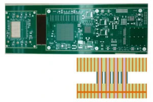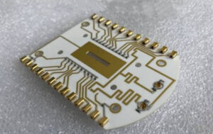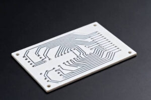
Choosing between DBC vs DPC ceramic PCB is mainly a choice between two different circuit-building priorities.
DBC—Direct Bonded Copper—bonds relatively thick copper foil directly to a ceramic substrate and is widely associated with high-current, high-power and thermal-management applications. DPC—Direct Plated Copper—creates the conductor through thin-film metallization followed by copper electroplating, making it more suitable when finer circuit features, smaller pads and higher dimensional precision are required.
In simple terms, DBC favors copper thickness and power handling, while DPC favors circuit precision and design density.
That does not mean one process is universally superior. A high-current power module and a compact optoelectronic module can both require ceramic substrates but demand completely different conductor structures.
The correct choice depends on the relationship between:
- Required copper thickness
- Current carrying demand
- Trace width and spacing
- Heat generation
- Component density
- Ceramic material
- Mechanical structure
- Production cost
For engineers evaluating a ceramic PCB, understanding these trade-offs before finalizing the layout can prevent unnecessary manufacturing compromises later.
The 60-Second DBC vs DPC Decision
Before looking at the manufacturing details, this table provides a practical starting point.
| Requirement | DBC | DPC |
| Thick copper conductors | Strong advantage | More limited |
| High current carrying | Strong advantage | Suitable depending on copper design |
| Fine traces and small spacing | More limited by thick-copper etching | Strong advantage |
| High circuit density | Moderate | Strong |
| Dimensional precision | Moderate to high depending on design | High |
| Power semiconductor modules | Strong fit | Application dependent |
| Fine-pitch electronic modules | Less suitable | Strong fit |
| Thermal spreading through copper | Excellent with thick copper | Good, but copper is generally thinner |
| Complex micro-scale patterns | Less favorable | More favorable |
| Main design priority | Power and thermal load | Precision and miniaturization |
If the design requires heavy current paths and substantial copper cross-sectional area, start by evaluating DBC. If it requires fine features and compact routing, start by evaluating DPC.
The next question is why these differences exist.
DBC and DPC Build the Copper Layer Differently
The final ceramic circuit may look similar from a distance, but the copper is created through fundamentally different manufacturing routes.
That process difference explains most of the differences in copper thickness, line resolution and application suitability.
How DBC Ceramic PCB Is Made
DBC stands for Direct Bonded Copper.
Instead of depositing copper gradually, DBC starts with copper foil.
In a typical DBC structure:
- A ceramic substrate is prepared.
- Copper foil is placed against the ceramic.
- The structure undergoes a controlled high-temperature bonding process.
- A copper-oxygen interfacial reaction creates a strong bond between copper and ceramic.
- The bonded copper is subsequently patterned to form the circuit.
Technical literature commonly describes DBC with copper layers in the hundred-micron range; one published characterization reports typical DBC copper around 127–500 μm. Exact capabilities depend on the substrate structure and manufacturing process.
The key point is not one fixed number.
It is that DBC begins with substantial copper foil, making thick conductive structures inherent to the technology.
That is why DBC has become strongly associated with:
- IGBT modules
- MOSFET power modules
- Power conversion
- Motor drives
- Automotive power electronics
- High-current industrial electronics
How DPC Ceramic PCB Is Made
DPC stands for Direct Plated Copper.
Rather than bonding a thick copper sheet to the ceramic, DPC generally begins by forming a very thin conductive seed layer on the ceramic surface.
A simplified process may include:
- Ceramic substrate preparation
- Vacuum metallization or sputtering
- Formation of a conductive seed layer
- Photolithographic pattern definition
- Copper electroplating
- Removal of unwanted seed material
- Surface finishing and subsequent processing
This combination of thin-film deposition, photolithography and electroplating allows the circuit geometry to be defined more precisely than would normally be practical when chemically removing very thick copper.
DPC achieves its main advantage by building copper selectively and precisely rather than starting with a thick copper foil and removing large amounts of material.
This makes it attractive for applications where line geometry is more important than maximum conductor thickness.
Copper Thickness Is the First Major Trade-Off
Copper thickness influences far more than the appearance of the PCB.
It directly affects:
- Electrical resistance
- Current carrying capability
- Voltage drop
- Joule heating
- Heat spreading
- Etching behavior
- Line resolution
- Mechanical stress
This creates the central DBC/DPC engineering trade-off.
Why DBC Is Better Suited to Thick Copper
Because DBC bonds copper foil directly to the ceramic, relatively thick copper can be integrated into the substrate.
A larger copper cross-sectional area reduces conductor resistance.
For a power circuit, this can be important when carrying:
- High continuous current
- Large switching current
- Motor drive current
- Battery power
- Inverter current
Thick copper also provides lateral heat spreading.
Heat generated underneath a semiconductor can spread through the copper before passing through the ceramic toward the cooling structure.
This combination of electrical conduction and thermal spreading is one reason DBC is widely used in high-power electronic substrates.
Why DPC Usually Uses Thinner Copper
DPC builds copper by electroplating.
Increasing conductor thickness therefore requires additional plating, and the copper geometry must remain controlled as the layer grows.
DPC can provide useful conductor thickness for many electronic applications, but its strongest reason for selection is normally not maximum copper thickness.
Its advantage is precision.
For this reason, specifying DPC simply because “plated copper sounds more advanced” is the wrong approach.
The actual question should be:
Does the circuit need more copper cross-section or more routing precision?
That distinction usually makes the choice clearer.
Why Thick Copper and Fine Lines Work Against Each Other
A useful way to understand DBC vs DPC ceramic PCB is to look at what happens during pattern formation.
Consider a thick copper layer that must be chemically etched.
The etchant does not remove copper only vertically.
Some lateral removal also occurs beneath the mask edge.
As copper becomes thicker, controlling this lateral etching becomes increasingly difficult.
This is often described as undercut.
Suppose a designer wants:
- Very thick copper
- Extremely narrow traces
- Extremely narrow spaces
- Nearly vertical conductor sidewalls
Those requirements begin to compete with each other.
The thicker the copper becomes, the more challenging it generally is to maintain very fine etched geometry and tight trace-to-space control.
That is not a defect unique to ceramic PCBs. It is a fundamental manufacturing consideration when patterning substantial metal thickness.
Why DPC Can Achieve Higher Circuit Precision
DPC approaches the circuit from the opposite direction.
Photolithography defines where the copper should grow, after which electroplating builds the conductor.
This provides greater control over small features and makes DPC attractive for:
- Narrow traces
- Fine spacing
- Small pads
- Dense routing
- Compact packages
- Fine-pitch devices
Some DPC processes are capable of line/space dimensions below 50 μm, although actual design rules vary by manufacturer, copper thickness, substrate size and process capability. (PCBONLINE)
The practical lesson is more important than the minimum published number:
DPC should be considered when conductor geometry and placement accuracy are more important than achieving very heavy copper.
A manufacturable design should always use the actual supplier’s DFM capability rather than treating a theoretical minimum line width as a production target.
DBC vs DPC: Copper Thickness and Precision Compared
| Design Characteristic | DBC Ceramic PCB | DPC Ceramic PCB |
| Copper formation | Bonded copper foil | Deposited seed layer + electroplating |
| Typical conductor character | Thick | Thin to medium |
| High-current capability | Excellent | Design dependent |
| Fine-line capability | Moderate | Excellent |
| Small pad capability | More restricted by thick copper | Strong |
| High-density routing | Moderate | Strong |
| Copper heat spreading | Strong | Lower because copper is usually thinner |
| Photolithographic precision | Patterning constrained by copper thickness | Major process advantage |
| Main manufacturing challenge | Thick-copper pattern definition and thermal stress | Plating uniformity and fine-feature process control |
| Best design direction | Power density | Circuit density |
This table should be used as a design direction—not as an absolute manufacturing specification.
Does DBC Have Better Thermal Performance Than DPC?
This question requires a more precise answer.
Both DBC and DPC use ceramic substrates, meaning the thermal performance of the board is strongly influenced by the ceramic material itself.
Common substrate options can include:
- Al2O3 alumina
- AlN aluminum nitride
- Other technical ceramics depending on process and application
Therefore, comparing a DBC board and a DPC board without knowing their ceramic materials is incomplete.
However, DBC often has a practical thermal advantage at the conductor level because it commonly uses thicker copper.
Thick copper can:
- Spread heat laterally
- Reduce conductor resistance
- Carry higher currents
- Reduce localized conductor heating
But the total thermal path also includes:
Semiconductor → attachment layer → copper → ceramic → backside interface → heat sink
If the ceramic or thermal interface dominates the total thermal resistance, simply increasing copper thickness may produce limited improvement.
For this reason, ceramic PCB design should evaluate the complete thermal stack rather than comparing only process names.
Current Carrying Capability: Where DBC Usually Leads
For high-current circuits, conductor cross-sectional area is critical.
Resistance can be considered conceptually as:
R = ρL / A
Where:
- R = conductor resistance
- ρ = copper resistivity
- L = conductor length
- A = conductor cross-sectional area
Increasing copper thickness increases cross-sectional area.
That reduces resistance for the same trace width and length.
Lower resistance means less resistive heating:
P = I²R
This is why copper thickness becomes increasingly important as current rises.
DBC is therefore particularly attractive where the PCB must simultaneously:
- Carry substantial current
- Transfer heat away from power devices
- Electrically isolate the circuit from the cooling structure
This combination appears frequently in power semiconductor modules.
DPC Solves a Different Problem: Packaging More Circuit Into Less Space
Not every ceramic PCB is carrying hundreds of amps.
Many applications use ceramic because they need:
- Thermal stability
- Electrical insulation
- Dimensional stability
- Heat transfer
- Compact packaging
At the same time, the circuit may require significantly finer geometry.
For example, one substrate could contain:
- Closely spaced LED dies
- Sensor elements
- Small bonding pads
- Dense control circuitry
- Fine wire-bonding features
Increasing copper thickness would not necessarily improve that design.
It could make routing more difficult.
DPC therefore fills the gap between the thermal and insulation benefits of ceramic substrates and the finer circuit requirements found in compact electronic packages.
Application Match: Where Each Process Makes Sense
Instead of choosing from a specification table alone, examine what the finished assembly actually needs to do.
Power Semiconductor Modules
Likely direction: DBC
Typical priorities include:
- High current
- Low conductor resistance
- Strong heat spreading
- Large power devices
- Reliable ceramic isolation
DBC’s thick copper structure aligns well with these requirements.
Applications may include:
- IGBT modules
- MOSFET modules
- Power converters
- Motor drives
- Inverters
High-Power LED Assemblies
Possible direction: DBC or DPC
The answer depends on the design.
A high-power LED module with significant current and thermal load may benefit from DBC.
A compact LED or optoelectronic assembly that requires fine pads and precise routing may instead favor DPC.
The decision cannot be made from “LED application” alone.
The heat density and circuit geometry must be evaluated together.
Laser and Optoelectronic Modules
Likely direction: DPC when fine geometry dominates
Optoelectronic assemblies can require:
- Small bonding areas
- Accurate conductor geometry
- Compact packaging
- Precise device positioning
DPC can be attractive because its process supports finer circuit features.
If power density becomes very high, however, the thermal design must still be evaluated separately.
Automotive Power Electronics
Likely direction: DBC for high-current power stages
Automotive power systems may combine:
- High current
- Significant thermal cycling
- Compact mechanical packaging
- High operating temperatures
DBC is therefore commonly associated with traction inverters, power modules and similar high-power assemblies.
Lower-power control or sensing circuits may have different requirements.
RF and High-Density Electronic Modules
Possible direction: DPC
When routing accuracy, pad dimensions or feature density becomes important, DPC deserves evaluation.
However, RF material selection also depends on electrical properties and circuit design.
Fine lines alone should not determine substrate choice.
Application Selection Table
| Application Requirement | DBC | DPC |
| IGBT power module | ★★★★★ | ★★ |
| High-current MOSFET module | ★★★★★ | ★★ |
| Motor drive power stage | ★★★★★ | ★★ |
| Power converter | ★★★★★ | ★★★ |
| High-power LED module | ★★★★ | ★★★★ |
| Fine-pitch LED array | ★★★ | ★★★★★ |
| Laser diode module | ★★★ | ★★★★★ |
| Compact optoelectronics | ★★ | ★★★★★ |
| Fine wire-bonding pattern | ★★★ | ★★★★★ |
| Dense small-pad circuit | ★★ | ★★★★★ |
The ratings indicate general process suitability rather than guaranteed performance for a specific design.
One Requirement Often Determines the Choice
A useful engineering method is to identify the requirement that cannot be compromised.
If the non-negotiable requirement is:
“We need much thicker copper.”
→ Evaluate DBC first.
“We need finer traces and smaller spaces.”
→ Evaluate DPC first.
“We need maximum current in a small power module.”
→ DBC is usually the stronger starting point.
“We need very accurate small pads for compact components.”
→ DPC is generally more suitable.
“We need both extremely thick copper and extremely fine lines.”
→ The layout requirements may need to be reconsidered.
This last situation is important.
Sometimes the correct engineering response is not to search for a manufacturing process that satisfies two conflicting extremes.
It is to change the circuit architecture.
Do Not Select DBC or DPC Before Choosing the Ceramic Material
DBC and DPC describe the copper metallization process.
They do not fully define the substrate.
The underlying ceramic remains a critical design variable.
For example, engineers may compare alumina with aluminum nitride depending on:
- Thermal conductivity
- Cost
- Mechanical requirements
- Thermal expansion
- Application temperature
A DBC alumina structure and a DBC AlN structure can have substantially different thermal behavior even though both use the same basic copper-bonding concept.
Similarly, DPC performance depends on the underlying ceramic.
This means there are actually two separate decisions:
Decision 1: Which ceramic material meets the thermal and mechanical requirements?
Decision 2: Which metallization process meets the copper thickness and circuit-resolution requirements?
Separating these decisions prevents confusion.
Five DFM Questions to Answer Before Sending Your Gerber Files
A supplier can evaluate a ceramic PCB much more effectively when the engineering priorities are known.
1. What Is the Required Copper Thickness?
Do not simply request “thick copper.”
Specify the target.
Copper thickness affects:
- Current capacity
- Etching
- Line width
- Spacing
- Cost
2. What Is the Minimum Trace and Space?
This requirement can immediately influence whether DBC or DPC is the more practical process.
Very fine geometry combined with thick copper should be reviewed before production.
3. What Current Must Each Critical Path Carry?
Provide actual operating current where possible.
This is more useful than selecting copper thickness only from a previous PCB design.
4. Where Is the Main Heat Source?
The supplier should understand:
- Component location
- Heat-source size
- Power dissipation
- Cooling direction
- Heat sink interface
This helps distinguish between conductor heating and semiconductor-generated heat.
5. What Assembly Process Will Be Used?
Ceramic circuit design may also interact with:
- Soldering
- Wire bonding
- Die attach
- Sintering
- Surface finish
- Mounting method
PCB fabrication should therefore be considered together with assembly requirements.
Cost: DBC Is Not Automatically More Expensive, and DPC Is Not Automatically Cheaper
A simple process-name comparison cannot reliably predict quotation price.
Final cost can depend on:
| Cost Driver | Why It Matters |
| Ceramic material | AlN and alumina have different material costs |
| Ceramic thickness | Influences raw material and processing |
| Copper thickness | Affects material use and manufacturing time |
| Fine line requirements | Increase process-control demands |
| Board dimensions | Affect panel utilization |
| Complex outlines | Increase machining requirements |
| Hole requirements | Ceramic machining may add processing |
| Tolerances | Tight tolerances increase manufacturing difficulty |
| Surface finish | Depends on assembly requirement |
| Quantity | Prototype and volume economics differ |
| Yield | Difficult combinations can increase production cost |
For procurement teams, the correct comparison is therefore not:
“Which technology is cheaper?”
It is:
“Which process produces our required structure with acceptable yield and without paying for capability we do not need?”
Common Selection Mistakes
Mistake 1: Assuming DBC Is Better Because It Handles More Power
A high-power capability is useful only when the application needs it.
If the circuit requires fine routing and moderate current, DPC may be the more appropriate technology.
Mistake 2: Choosing DPC Only Because It Has Better Precision
Precision should also match the actual layout.
If the minimum trace and spacing are relatively large while current requirements are high, paying for a fine-line process provides little benefit.
Mistake 3: Ignoring Copper Thickness During Layout
Using the same minimum trace width for thin copper and very thick copper can cause manufacturability problems.
Copper thickness should be considered before routing is finalized.
Mistake 4: Treating Ceramic Thermal Conductivity as the Entire Thermal Design
The thermal path includes copper, ceramic, solder, thermal interface materials and the heat sink.
No single material property represents total system thermal resistance.
How to Request a Useful DBC or DPC Ceramic PCB Quotation
Rather than sending only Gerber files and asking for a unit price, include the major performance requirements.
A useful RFQ can contain:
- Ceramic type
- Ceramic thickness
- Copper thickness
- Minimum trace width
- Minimum spacing
- Board dimensions
- Number and size of holes
- Surface finish
- Operating voltage
- Maximum current
- Thermal load
- Critical dimensional tolerances
- Prototype quantity
- Estimated production quantity
If the process has not yet been selected, provide the performance requirements instead of forcing either DBC or DPC into the RFQ.
A ceramic PCB manufacturer can then evaluate which process is more compatible with the design.
DBC vs DPC: Final Engineering Decision
The most useful distinction between DBC vs DPC ceramic PCB is not simply how the two processes are manufactured.
It is what each process allows the designer to prioritize.
DBC starts from substantial copper foil and is therefore well suited to designs where conductor thickness, current carrying capability and power-module thermal management are critical.
DPC builds copper using metallization and electroplating, making it particularly useful when circuit precision, smaller pads and fine routing features are the dominant requirements.
Choose DBC when the design is constrained primarily by current and power density. Choose DPC when it is constrained primarily by line geometry and circuit density.
For designs that sit between those two extremes, the decision should be made using actual copper thickness, line/space, thermal load and assembly requirements rather than application name alone.
Mars-PCB provides ceramic PCB manufacturing solutions for projects involving different ceramic substrates and circuit requirements. Providing your stack-up, copper thickness, minimum line/space and operating conditions allows the design to be evaluated from both performance and manufacturability perspectives.
You can also review the broader Mars-PCB PCB manufacturing capabilities when the project includes multiple PCB technologies or requires manufacturing evaluation beyond the ceramic substrate itself.
FAQ
What is the main difference between DBC and DPC ceramic PCB?
DBC bonds relatively thick copper foil directly to ceramic, while DPC forms a thin metal seed layer and builds copper through electroplating. DBC is generally better suited to high-current thick-copper designs, while DPC offers advantages for fine-line, high-precision circuits.
Which has thicker copper, DBC or DPC ceramic PCB?
DBC generally supports substantially thicker copper conductors because the process starts with copper foil. DPC builds copper through electroplating and is normally selected more for circuit precision than maximum copper thickness.
Is DPC ceramic PCB better for fine lines?
Yes, DPC is generally more suitable for fine traces, narrow spacing and small pads because photolithography and plating provide better control of fine circuit geometry than patterning very thick bonded copper.
Is DBC ceramic PCB better for high-current applications?
DBC is commonly preferred for high-current power electronics because its thick copper conductors provide a larger current-carrying cross-section and strong lateral heat spreading.
Does DBC have better thermal conductivity than DPC?
Not automatically. Ceramic material strongly affects through-plane thermal conductivity. However, the thicker copper typically used in DBC can improve lateral heat spreading and reduce conductor resistance.
Can both DBC and DPC use aluminum nitride ceramic?
Depending on manufacturing capability, both technologies can be used with ceramic materials such as AlN. Process availability and design limits should be confirmed with the manufacturer.
Which is better for power electronics: DBC or DPC?
For high-current power modules, DBC is generally the stronger starting point. DPC may be more appropriate when the electronic module requires finer conductor geometry, smaller pads or greater routing density.
How should I choose between DBC and DPC ceramic PCB?
Compare four requirements first: copper thickness, operating current, minimum line/space and thermal load. Thick copper and high current generally favor DBC, while fine lines and higher circuit density generally favor DPC.