The primary difference between DBC (Direct Bonded Copper) and DPC (Direct Plated Copper) ceramic PCBs lies in their manufacturing process and application precision. DBC uses a high-temperature eutectic reaction to bond thick copper to the ceramic, offering superior thermal conductivity and bonding strength for high-power, high-reliability applications. Conversely, DPC utilizes thin-film sputtering and photolithography, providing high-precision trace definitions and miniaturization capabilities, making it the preferred choice for high-frequency circuits and dense electronic packaging.
As the demand for high-performance electronics grows, the role of ceramic substrates in thermal management and signal integrity has become critical. Selecting between DBC and DPC substrates can significantly impact the reliability, cost, and functional limitations of a power module or LED array. This guide explores the technical nuances, manufacturing differences, and selection criteria to help engineers make informed decisions.
Understanding DBC (Direct Bonded Copper) Technology
DBC, or Direct Bonded Copper, is a mature technology primarily used in high-power applications. The process involves bonding a solid copper sheet directly to a ceramic substrate—typically Alumina (Al₂O₃) or Aluminum Nitride (AlN)—through a high-temperature eutectic reaction. This process takes place at temperatures slightly below the melting point of copper, allowing the copper to chemically bond with the oxygen-doped ceramic surface.
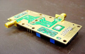
The hallmark of DBC is its mechanical robustness. Because it uses thick copper foils (ranging from 0.1mm to 0.6mm), the heat dissipation capacity is exceptional, handling high currents without thermal throttling. This makes DBC the industry standard for power modules, electric vehicle (EV) inverters, and high-current rectifiers where mechanical stress and thermal cycling are intense. However, due to the nature of etching thick copper, trace precision is generally lower compared to other methods, limiting its use in highly complex, miniaturized circuitry.
Understanding DPC (Direct Plated Copper) Technology
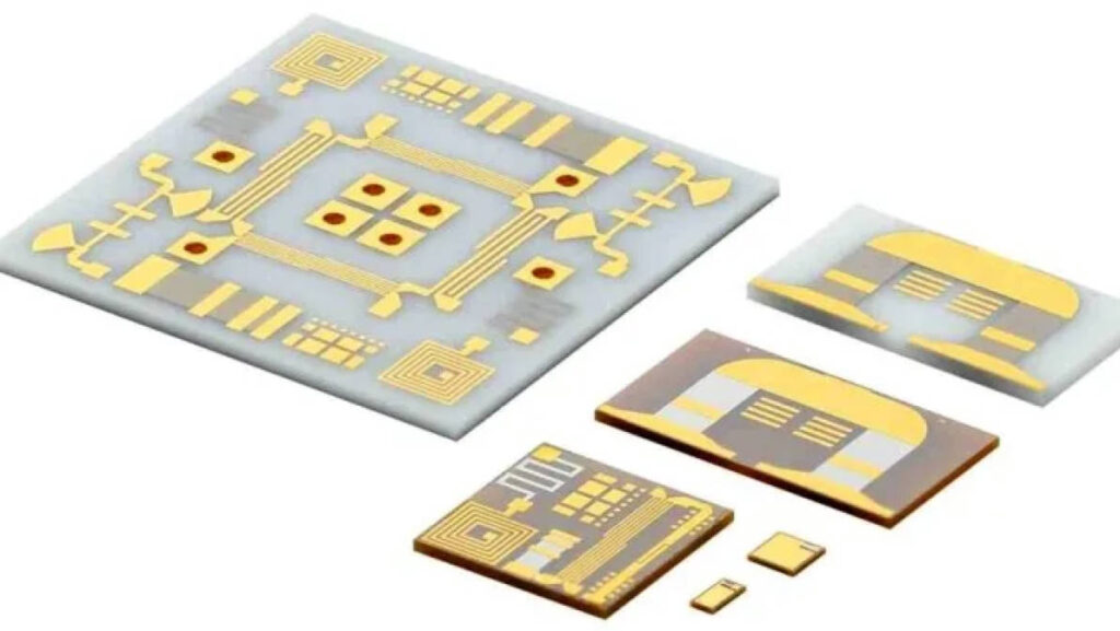
DPC, or Direct Plated Copper, represents the intersection of thin-film technology and printed circuit board fabrication. Unlike DBC, DPC does not use physical bonding of a copper foil. Instead, it employs vacuum sputtering (thin-film deposition) to lay down a seed layer of copper, followed by electroplating to build the desired thickness. This process is governed by photolithography, the same technology used in semiconductor wafer manufacturing.
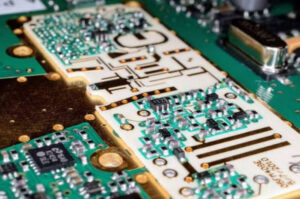
The core advantage of DPC is precision. Because it relies on photolithographic imaging, DPC can achieve extremely fine lines and narrow spacing, allowing for high-density interconnects. The surface of a DPC board is remarkably flat and smooth, which is critical for wire bonding and soldering small surface-mount components. While historically considered to have lower bonding strength than DBC, modern advancements in surface preparation have significantly closed this gap, making DPC the go-to solution for high-frequency communication modules, laser diodes, and advanced LED packaging.
Comparative Analysis: DBC vs. DPC
To differentiate effectively, we must evaluate the manufacturing methods and performance characteristics. The following table summarizes the technical trade-offs:
| Feature | DBC (Direct Bonded Copper) | DPC (Direct Plated Copper) |
|---|---|---|
| Manufacturing Method | High-temp eutectic bonding | Vacuum sputtering + Electroplating |
| Copper Thickness | Thick (up to 0.6mm+) | Thin (typically 10um – 100um) |
| Pattern Precision | Low (Etching limitations) | High (Photolithography) |
| Thermal Resistance | Excellent | Good |
| Bonding Strength | Very High | Moderate to High |
| Primary Application | Power Electronics, EV, IGBT | RF, Sensors, High-Density LED |
When analyzing these differences, it becomes clear that the choice is often dictated by the specific requirements of the current and signal path. If your design requires managing extreme heat flux for high-power switching, the structural advantage of thick copper in DBC is difficult to beat. If your design requires complex, dense, and miniaturized circuitry where thermal load is secondary to signal integrity, DPC offers superior geometric control.
Which Should You Choose? Selection Criteria
Selecting the appropriate substrate requires balancing thermal, electrical, and physical requirements. Consider the following decision framework:
1. Evaluate Current and Thermal Requirements
If your circuit involves massive power throughput—such as power management integrated circuits (PMICs) or motor drives—prioritize DBC. The thermal expansion coefficient of the thick copper in DBC, when matched properly with the ceramic, manages thermal shock effectively under high-load conditions.
2. Analyze Trace Density and Signal Frequency
If you are designing high-frequency RF modules, antennas, or compact sensors, DPC is the clear winner. The photolithographic process ensures consistent impedance control and allows for tighter component spacing, which is essential for reducing parasitic inductance in high-speed circuits.
3. Consider Surface Finish Requirements
DPC offers a flat, polished surface finish ideal for precision wire bonding. If your assembly process requires reliable Au/Sn (gold-tin) eutectic bonding or high-density wire bonding, DPC provides a more predictable and consistent contact interface compared to the relatively coarser etched surface of DBC.
Future Trends in Ceramic PCB Manufacturing
As power electronics push toward smaller footprints and higher power densities (the “More Moore” vs. “More than Moore” trend), the distinction between DBC and DPC is beginning to blur. Manufacturers are now experimenting with hybrid processes—such as plating onto DBC-like structures or using advanced laser activation for direct metallization—to achieve the best of both worlds: the thermal ruggedness of DBC and the precision of DPC. Staying updated with these material science advancements is essential for engineers aiming to future-proof their designs.