High frequency PCB materials should be selected based on operating frequency, dielectric constant, dissipation factor, thermal stability, moisture absorption, copper foil type, stackup structure, and manufacturability. The right substrate helps reduce signal loss, maintain controlled impedance, improve phase stability, and support reliable RF or microwave circuit performance.
For standard PCBs, FR4 is often enough for many digital, analog, or power applications. However, RF and microwave circuits are more sensitive to material behavior. At higher frequencies, the PCB substrate is no longer just a mechanical support. It becomes part of the signal transmission path.
This is why high frequency PCB material selection must be done carefully before fabrication. A material with the wrong Dk, high Df, unstable thickness, excessive moisture absorption, or unsuitable copper roughness can cause insertion loss, impedance mismatch, phase drift, poor antenna efficiency, or inconsistent test results.
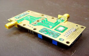
Mars-PCB supports high-frequency PCB manufacturing for RF, microwave, communication, radar, antenna, and other high-frequency applications. For material-sensitive projects, early review of substrate, stackup, impedance, and fabrication requirements can help reduce prototype and production risk.
What Are High Frequency PCB Materials?
High frequency PCB materials are substrates designed to support stable signal transmission at RF, microwave, or other high-frequency ranges. These materials usually provide better dielectric stability, lower signal loss, and improved performance consistency compared with standard PCB materials.
Common high-frequency PCB material categories include:
- Low-loss FR4 variants
- PTFE-based laminates
- Ceramic-filled PTFE composites
- Hydrocarbon ceramic laminates
- Rogers-type high-frequency materials
- Taconic-type RF materials
- LCP materials
- Polyimide materials
- Low-loss prepregs for multilayer RF boards
A high-frequency PCB substrate should not be selected by material name alone. It should be selected according to the circuit’s frequency, loss budget, impedance requirements, thermal environment, mechanical structure, and cost target.
Why Substrate Selection Matters in RF and Microwave PCBs
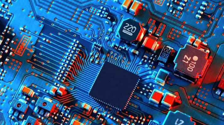
In RF and microwave circuits, the PCB material directly affects electrical performance. The substrate influences signal speed, impedance, insertion loss, phase behavior, crosstalk, thermal reliability, and manufacturing repeatability.
If the substrate is not suitable, the circuit may experience:
- Higher insertion loss
- Poor impedance matching
- Signal reflection
- Reduced antenna performance
- Lower RF output efficiency
- Phase instability
- Thermal expansion mismatch
- Moisture-related performance drift
- Prototype-to-production variation
For example, a wireless communication board may pass basic electrical testing but still perform poorly in RF testing if the material has excessive dielectric loss. A radar or antenna board may also show frequency shifts if the dielectric constant is not stable enough for the design.
For this reason, high frequency PCB materials should be chosen together with the stackup, impedance target, trace geometry, copper profile, and manufacturing process.
Key Material Properties for High-Frequency PCB Substrates
Dielectric Constant, or Dk
Dielectric constant, commonly called Dk, describes how much the substrate slows electromagnetic signal propagation compared with air. In PCB design, Dk affects signal velocity, impedance, wavelength, trace width, and circuit size.
A lower Dk can help reduce parasitic capacitance and allow wider traces for the same impedance. A higher Dk can help make circuits more compact, but it may require tighter manufacturing control.
When reviewing Dk, engineers should consider:
| Dk Factor | Why It Matters |
| Nominal Dk | Used for impedance and transmission-line calculation |
| Dk tolerance | Affects consistency between design and fabricated board |
| Dk stability over frequency | Important for broadband or microwave circuits |
| Dk stability over temperature | Important for harsh or high-power environments |
| Effective Dk | Influenced by copper, solder mask, stackup, and field distribution |
Dk is important, but it should never be the only criterion for choosing high frequency PCB materials. A material with the desired Dk may still have high loss, poor thermal performance, high moisture absorption, or difficult fabrication requirements.
Dissipation Factor, or Df
Dissipation factor, also called loss tangent or Df, measures dielectric loss. In simple terms, it indicates how much signal energy is absorbed by the substrate.
For high-frequency and microwave circuits, Df is one of the most important material properties because dielectric loss typically becomes more significant as frequency increases.
A lower Df can help reduce insertion loss, especially in:
- Long RF transmission lines
- Microwave circuits
- Antenna feed networks
- RF filters
- High-frequency communication modules
- Radar boards
- Satellite communication systems
However, the lowest Df material is not always the right choice. Cost, process compatibility, availability, thermal stability, copper type, and mechanical requirements must also be considered.
Thermal Stability and CTE
CTE means coefficient of thermal expansion. It describes how much a material expands or contracts with temperature. In high-frequency PCB manufacturing, CTE affects dimensional stability, plated through-hole reliability, layer registration, and long-term reliability.
Thermal stability is especially important for:
- RF power amplifiers
- Aerospace electronics
- Automotive radar
- Industrial wireless equipment
- High-power microwave modules
- Outdoor communication devices
- Boards exposed to thermal cycling
If the material expands too much or behaves differently from copper, vias and plated holes may experience stress. In multilayer boards, thermal mismatch between different materials can also create reliability risks.
Moisture Absorption
Moisture absorption is often underestimated in PCB material selection. When a substrate absorbs moisture, its dielectric properties may change. This can affect impedance, loss, and reliability.
Low moisture absorption is useful for:
- Outdoor communication equipment
- Aerospace and defense electronics
- Automotive electronics
- High-humidity environments
- Precision RF applications
- Long-life industrial systems
For RF and microwave circuits, even small dielectric changes may influence performance. This is why moisture absorption should be reviewed together with Dk, Df, temperature range, and operating environment.
Copper Foil Type and Roughness
At high frequencies, current tends to flow near the conductor surface due to the skin effect. As frequency increases, copper surface roughness can contribute more to conductor loss.
Rougher copper can improve adhesion, but it may increase high-frequency loss. Smoother copper can help reduce conductor loss, but it must still support reliable lamination and fabrication.
Common copper-related factors include:
| Copper Factor | Impact on High-Frequency PCB Performance |
| Copper thickness | Affects current capacity, impedance, and etching control |
| Copper roughness | Influences conductor loss at high frequencies |
| Copper profile | Affects signal loss and manufacturability |
| Plating thickness | Can influence final trace geometry and impedance |
| Trace edge quality | Affects RF transmission-line consistency |
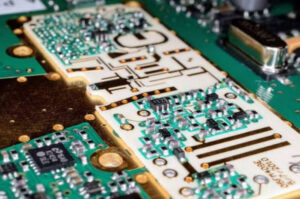
For RF and microwave boards, copper is not only a conductor; its surface profile can affect insertion loss and signal consistency.
Common Types of High-Frequency PCB Materials
Standard FR4
FR4 is widely used in standard PCB manufacturing because it is cost-effective, available, and easy to process. However, standard FR4 is not always suitable for high-frequency applications because it may have higher dielectric loss and less stable Dk than specialized RF materials.
FR4 may be acceptable for:
- Low-cost prototypes
- Moderate-speed digital circuits
- Some lower-frequency RF designs
- Non-critical RF support areas
- Cost-sensitive products with relaxed loss requirements
FR4 may not be suitable for:
- Microwave circuits
- Low-loss RF transmission lines
- Precision antennas
- Radar modules
- High-frequency filters
- Phase-sensitive circuits
Low-Loss FR4
Low-loss FR4 materials are designed to offer better dielectric performance than standard FR4 while maintaining relatively familiar fabrication characteristics. They can be useful for some high-speed digital or moderate-frequency RF applications.
Low-loss FR4 can be a practical choice when:
- Cost must be controlled
- The frequency is not extremely high
- The RF path is short
- The insertion loss budget is moderate
- The design does not require very tight phase stability
However, low-loss FR4 should still be evaluated carefully against the required Dk, Df, thickness tolerance, and operating frequency.
PTFE-Based Materials
PTFE-based materials are commonly used in demanding RF and microwave applications because they can provide very low dielectric loss and stable electrical behavior.
PTFE materials are often considered for:
- Microwave circuits
- Antenna systems
- RF filters
- High-frequency communication devices
- Radar modules
- Satellite communication boards
- Low-loss transmission lines
The tradeoff is that PTFE-based materials can be more complex to fabricate than standard FR4. They may require specialized lamination, drilling, surface treatment, and process control.
Ceramic-Filled PTFE
Ceramic-filled PTFE materials combine the low-loss benefits of PTFE with improved dimensional and thermal stability. These materials are often used when both RF performance and mechanical stability are important.
They may be suitable for:
- RF power applications
- Microwave modules
- Automotive radar
- Aerospace electronics
- High-reliability communication systems
- Circuits requiring better thermal stability
The final decision depends on frequency, power level, stackup, thermal environment, and manufacturing capability.
Rogers-Type High-Frequency Materials
Rogers-type materials are widely used in RF and microwave PCB applications. Different material families are designed for different combinations of Dk, Df, thermal behavior, cost, and fabrication compatibility.
They are commonly used in:
- RF modules
- Microwave circuits
- Antennas
- Radar systems
- Communication equipment
- High-frequency test boards
- Power amplifiers
When selecting a Rogers-type material, engineers should not only compare material names. They should check the specific Dk, Df, thickness, copper type, availability, and fabrication requirements.
Taconic-Type RF Materials
Taconic-type materials are also used in RF and microwave PCB applications. They may be selected for low-loss performance, PTFE-based structures, or specific microwave design needs.
As with other RF materials, selection should be based on electrical performance, mechanical requirements, thermal behavior, cost, and manufacturability.
LCP and Polyimide Materials
LCP and polyimide materials may be used in specialized high-frequency or flexible PCB applications. Polyimide is known for thermal resistance, while LCP can offer good electrical properties for certain high-frequency and flexible designs.
These materials may be relevant for:
- Flexible RF circuits
- Compact wireless modules
- High-temperature environments
- Wearable or compact electronic devices
- Hybrid rigid-flex structures
Material selection should consider bend requirements, thermal exposure, dielectric performance, and fabrication constraints.
Low-Loss Prepregs
For multilayer high-frequency PCBs, prepreg selection is also important. Even if the core material performs well, the bonding material can affect loss, impedance, and reliability.
Low-loss prepregs are used to bond layers while maintaining better electrical performance in multilayer RF and microwave boards.
High-Frequency PCB Material Comparison
| Material Type | Main Advantages | Common Limitations | Typical Use Cases |
| Standard FR4 | Low cost, easy to fabricate, widely available | Higher loss, less stable for demanding RF applications | General electronics, low-cost prototypes, non-critical areas |
| Low-loss FR4 | Better loss performance than standard FR4, familiar process | May not be enough for microwave or low-loss RF circuits | High-speed digital, moderate RF, cost-sensitive projects |
| PTFE-based laminates | Very low dielectric loss, good RF performance | More complex fabrication, higher cost | Microwave circuits, antennas, radar, low-loss RF paths |
| Ceramic-filled PTFE | Low loss with improved thermal and dimensional stability | Requires careful fabrication control | RF power, automotive radar, aerospace, microwave modules |
| Rogers-type materials | Broad RF/microwave options, stable electrical properties | Material selection and availability need review | RF modules, microwave circuits, antennas, communication devices |
| Taconic-type materials | RF and microwave material options | Processing and availability depend on material type | Microwave designs, RF transmission structures |
| LCP | Useful for some high-frequency flexible applications | Specialized processing and design requirements | Flexible RF circuits, compact wireless modules |
| Polyimide | High temperature resistance, flexible PCB compatibility | Electrical performance varies by grade | High-temperature and flexible applications |
| Low-loss prepreg | Supports multilayer RF stackups | Must match core materials and lamination process | Multilayer high-frequency PCBs |
How to Choose the Right High-Frequency PCB Substrate
Step 1: Define the Operating Frequency
The operating frequency is one of the first parameters to review. A material that works well at lower RF frequencies may not perform well at microwave or millimeter-wave frequencies.
Designers should define:
- Fundamental frequency
- Harmonics
- Bandwidth
- Signal path length
- Acceptable insertion loss
- Phase stability requirements
- Power level
- Environmental conditions
The higher the frequency and the tighter the loss budget, the more important low-loss material selection becomes.
Step 2: Determine the Loss Budget
The loss budget defines how much signal attenuation the system can tolerate. If the PCB is part of a long RF path, antenna feed network, or high-performance microwave circuit, dielectric loss and conductor loss should be carefully reviewed.
Loss budget considerations include:
- Dielectric loss from Df
- Conductor loss from copper
- Copper roughness loss
- Via transition loss
- Connector launch loss
- Reflection loss from impedance mismatch
If the design has a strict loss budget, using a low Df PCB material may be necessary.
Step 3: Review Impedance Requirements
Many RF designs use 50-ohm transmission lines, while some applications may use other impedance values. The substrate Dk, dielectric thickness, copper thickness, and trace width all influence impedance.
A material should be selected together with the stackup. If the selected substrate requires extremely narrow or wide traces that are difficult to manufacture, another material or thickness may be more practical.
Step 4: Evaluate Thermal and Environmental Conditions
High-frequency boards may operate in outdoor, automotive, aerospace, industrial, or high-power environments. Material selection should consider temperature range, thermal cycling, humidity, and power dissipation.
For harsh environments, stability can be as important as initial RF performance.
Step 5: Check Fabrication Compatibility
A material may look ideal in the datasheet but still create manufacturing challenges. Before finalizing the design, review whether the PCB manufacturer can support the required material, thickness, copper foil, stackup, drilling, lamination, and surface finish.
Mars-PCB provides high-frequency PCB fabrication support for customers who need material and stackup review before manufacturing.
Material Selection by Application
| Application | Material Selection Focus |
| 5G communication modules | Low Df, stable Dk, controlled impedance, multilayer compatibility |
| Radar systems | Low loss, phase stability, thermal stability, reliable fabrication |
| Antenna PCBs | Stable Dk, low loss, thickness consistency, predictable impedance |
| RF power amplifiers | Thermal performance, low loss, copper thickness, dimensional stability |
| Satellite communication | Low loss, reliability, thermal stability, environmental resistance |
| High-speed digital with RF sections | Hybrid stackup, low-loss FR4 or RF materials for critical layers |
| Flexible RF circuits | LCP, polyimide, or other flexible RF-compatible materials |
| Microwave filters | Tight Dk tolerance, low Df, precise trace geometry, stable stackup |
Common Mistakes in High-Frequency PCB Material Selection
Mistake 1: Choosing Material Only by Price
Lower material cost may increase total project cost if the board fails RF testing, requires redesign, or causes inconsistent production results.
Mistake 2: Looking Only at Dk
Dk affects impedance and circuit size, but it does not tell the whole story. Df, copper roughness, thermal stability, moisture absorption, and manufacturability also matter.
Mistake 3: Ignoring Copper Foil
At high frequencies, conductor loss can become significant. Copper roughness should be reviewed for low-loss RF and microwave applications.
Mistake 4: Using Standard FR4 Without Loss Analysis
FR4 may be acceptable in some applications, but it should not be selected automatically for demanding high-frequency circuits.
Mistake 5: Finalizing Layout Before Stackup Confirmation
The stackup affects trace width, impedance, spacing, and manufacturability. It should be confirmed before the final layout is completed.
Mistake 6: Not Discussing Material Availability Early
Some high-frequency materials may have longer procurement lead times. Material availability should be checked before urgent prototype or production planning.
What Information Should You Provide for Material Selection?
To help a PCB manufacturer recommend or verify high-frequency PCB materials, provide as much project information as possible.
| Information | Why It Helps |
| Operating frequency | Determines required RF performance |
| Application type | Helps evaluate material priorities |
| Loss budget | Supports low-loss material selection |
| Target impedance | Guides stackup and trace geometry |
| Board thickness | Affects mechanical and electrical design |
| Layer count | Determines stackup complexity |
| Copper weight | Affects current, loss, and etching |
| Thermal environment | Helps assess CTE and thermal stability |
| Humidity or outdoor use | Helps evaluate moisture absorption |
| Preferred material | Allows manufacturer to check availability |
| Approved alternatives | Can reduce lead time and cost |
| Surface finish | Affects assembly and reliability |
| Quantity and schedule | Helps plan prototype or production |
For projects where the material is not fixed, engineers can discuss requirements with Mars-PCB before finalizing the PCB layout.
How to Choose a High-Frequency PCB Manufacturer for Material-Sensitive Projects
A suitable high-frequency PCB manufacturer should be able to support more than basic board fabrication. Material-sensitive RF and microwave projects require engineering communication before production.
When evaluating a supplier, consider:
| Supplier Capability | Why It Matters |
| Experience with RF PCB materials | Helps avoid material and processing mistakes |
| Material availability support | Affects lead time and cost |
| Stackup review | Ensures material, thickness, and impedance work together |
| Controlled impedance capability | Important for RF transmission lines |
| Lamination process control | Affects dielectric stability and reliability |
| Copper profile understanding | Helps manage conductor loss |
| DFM review | Identifies fabrication risks before production |
| Prototype and production support | Supports development from sample to volume build |
A reliable manufacturer should be able to review the material, stackup, trace geometry, impedance target, via structure, and surface finish before fabrication begins.
Mars-PCB offers custom high-frequency PCB manufacturing for RF and microwave applications, helping customers evaluate materials, stackups, and fabrication requirements for high-frequency circuit boards.
FAQ: High-Frequency PCB Materials
1. What are high frequency PCB materials?
High frequency PCB materials are substrates designed for RF, microwave, wireless, radar, antenna, and other high-frequency circuits. They usually offer lower loss, more stable dielectric properties, and better signal integrity than standard PCB materials.
2. What is the best substrate for RF PCB design?
There is no single best substrate for every RF PCB design. The right material depends on operating frequency, insertion loss budget, Dk, Df, thermal stability, copper foil type, stackup, cost, and manufacturability.
3. Is FR4 suitable for high frequency PCB applications?
FR4 may be suitable for some lower-frequency or cost-sensitive designs, but standard FR4 is often not ideal for demanding RF or microwave applications. Low-loss FR4 or specialized RF materials may be needed when signal loss and impedance stability are critical.
4. Why is Df important in high frequency PCB materials?
Df, or dissipation factor, indicates dielectric loss. A lower Df helps reduce signal attenuation, especially at higher frequencies. This is why low Df PCB materials are often used in RF and microwave circuits.
5. How does Dk affect high-frequency PCB design?
Dk affects signal speed, impedance, wavelength, and trace width. A stable Dk helps maintain predictable RF behavior and improves consistency between design simulation and fabricated boards.
6. What PCB material is used for microwave circuits?
Microwave circuits commonly use low-loss materials such as PTFE-based laminates, ceramic-filled PTFE, Rogers-type materials, Taconic-type materials, and other RF-grade substrates. The final choice depends on frequency, loss budget, stackup, and cost.
7. How do I choose low loss PCB material for RF circuits?
To choose low loss PCB material for RF circuits, review operating frequency, Dk, Df, copper roughness, dielectric thickness, thermal stability, moisture absorption, impedance requirements, and manufacturing compatibility.
Conclusion
Choosing the right high frequency PCB materials is one of the most important decisions in RF and microwave circuit development. The substrate affects signal loss, impedance, phase stability, thermal reliability, moisture behavior, and manufacturing consistency.
A good material choice should balance electrical performance, mechanical reliability, fabrication feasibility, lead time, and cost. Engineers should avoid selecting materials based only on brand name, Dk value, or price. Instead, they should evaluate Dk, Df, copper foil, CTE, moisture absorption, stackup, application environment, and supplier capability together.
If your project involves RF modules, microwave circuits, antennas, radar boards, satellite communication, or high-frequency communication equipment, Mars-PCB can support your material review and fabrication needs through high-frequency PCB manufacturing services.