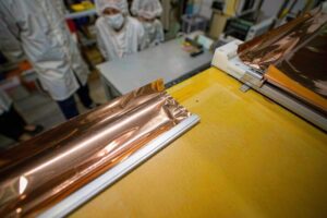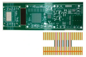
Copper foil roughness increases RF PCB insertion loss because high-frequency current flows close to the conductor surface and must follow its microscopic peaks, valleys and treatment nodules. This increases the effective current path and AC resistance compared with an ideally smooth conductor.
As frequency rises and skin depth becomes comparable to or smaller than the copper surface profile, roughness can become a significant part of total conductor loss.
The effect is especially important in long RF transmission lines, millimeter-wave circuits, thin dielectric constructions and designs already using a low-loss laminate. In these applications, selecting smooth copper foil and controlling the fabricator’s bonding treatment can preserve channel margin that would otherwise be lost.
However, copper roughness should not be evaluated as an isolated data-sheet number. Its actual effect depends on frequency, trace geometry, dielectric thickness, transmission-line structure, foil treatment, fabrication process and the model used in simulation.
A useful high-frequency PCB fabrication review should therefore examine the complete copper–dielectric interface rather than only the laminate’s nominal dissipation factor.
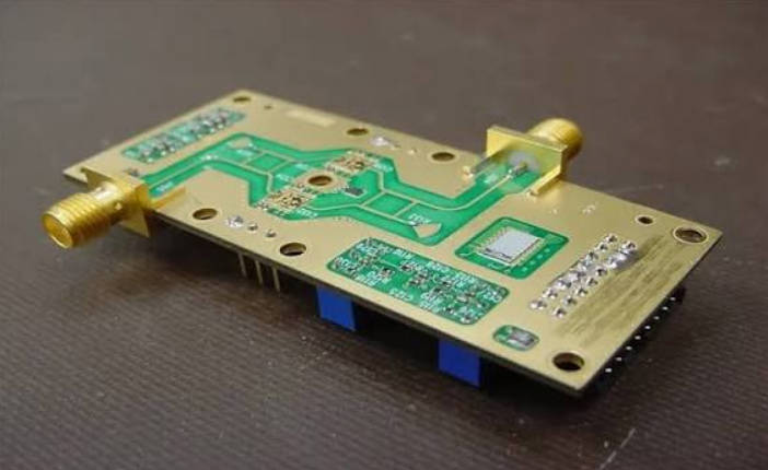
The Roughness Problem Begins Where the Current Flows
At direct current or relatively low frequencies, current is distributed through much of the copper conductor’s cross-section. As frequency increases, electromagnetic fields force more current toward the conductor surface. This is known as the skin effect.
Skin depth can be expressed approximately as:
δ = √[2 ÷ (ωμσ)]
where:
- δ is skin depth;
- ω is angular frequency;
- μ is magnetic permeability;
- σ is electrical conductivity.
For copper under typical assumptions, skin depth is approximately 2.1 μm at 1 GHz and falls below 1 μm by around 10 GHz. At these frequencies, a copper surface profile several micrometers high is no longer a minor geometric imperfection relative to the region carrying most of the current.
A simplified smooth-conductor model assumes that current travels along a flat surface. Real PCB copper contains microscopic nodules and valleys that can force surface current through a more complex path.
This produces two related effects:
- The effective path travelled by the current becomes longer.
- The apparent surface resistance becomes greater than the smooth-copper calculation predicts.
The result appears in the measured S-parameters as additional attenuation.
Copper roughness does not create a separate signal mechanism; it increases the conductor-loss portion of the existing transmission line.
From Microns to Decibels: The Loss Chain
The relationship between copper roughness and insertion loss can be understood as a four-stage chain.
Stage 1: Current Becomes Confined to the Surface
As frequency increases, the conducting region becomes progressively shallower. A larger percentage of the current interacts directly with the microscopic surface profile.
Stage 2: The Surface Is Not Electrically Flat
Copper foil is intentionally textured to improve adhesion between the conductor and resin. Electrodeposited foil may also contain a natural matte-side profile created during production.
The current must flow across this irregular surface rather than through a perfectly straight plane.
Stage 3: Effective AC Resistance Increases
The more complex current path and local field concentration increase conductor attenuation. The effect cannot always be represented accurately by simply reducing the bulk conductivity of copper.
Models such as the Hammerstad correction and Huray snowball model were developed to approximate how surface texture modifies conductor loss. The Huray model represents the rough surface through groups of conductive spheres and relates their surface area to the additional loss. (IEEE Xplore)
Stage 4: Measured S21 Becomes More Negative
Insertion loss is commonly evaluated through S21. For a passive RF transmission line, a more negative S21 magnitude indicates that less signal power reaches the output.
The measured loss contains more than copper roughness. It can include:
- dielectric loss;
- smooth-conductor skin-effect loss;
- roughness-related conductor loss;
- radiation and leakage;
- connector and launch loss;
- impedance discontinuities;
- via and transition loss.
Copper roughness is therefore one contributor to the complete measurement, not the only explanation for poor S21.
A Trace Has More Than One Copper Surface
One of the most common design oversimplifications is to treat the copper trace as though it has a single roughness value.
An internal stripline conductor can have different surface conditions on different sides.
The Foil Bonding Side
This is the side originally bonded to the laminate resin. Depending on the foil type, it may contain electrodeposited nodules, reverse treatment or another adhesion-promoting structure.
The Fabricator-Treated Side
After an inner-layer circuit is etched, the exposed copper must bond to the next prepreg layer during multilayer lamination. The PCB fabricator therefore applies an oxide or oxide-alternative process.
That treatment can change the surface profile and introduce additional roughness even when the original foil is relatively smooth.
Published test work has shown that inner-layer surface treatment can measurably affect insertion loss independently of the initial foil type. One study reported that a lower-roughness surface treatment reduced insertion loss by approximately 0.42 dB over a 16-inch line at 10 GHz compared with a conventional alternative-oxide treatment. The result is specific to that test construction, but it demonstrates why the fabrication process belongs in the loss model.
Specifying VLP copper is incomplete if the opposite side of the trace is later roughened by an aggressive bonding treatment.
For stripline circuits, both copper–dielectric interfaces should be considered. For microstrip and grounded coplanar structures, the field distribution may make one interface more influential than another, but the full transmission-line geometry still needs to be modelled.
Standard, VLP and Ultra-Low-Profile Copper
Copper foil terminology can be confusing because names, measurement methods and supplier definitions are not always completely consistent.
The following ranges are useful as general industry references, not universal acceptance limits.
| Copper Foil Category | Indicative Surface Profile | Typical RF Consideration |
| Standard electrodeposited copper | Approximately 7–8 μm Rz in some industry references | Greater roughness-related conductor loss at high frequencies |
| Low-profile copper | Lower profile than standard foil | Moderate loss improvement, depending on treatment and structure |
| VLP copper | Commonly around 3–5 μm Rz in historical classification examples | Frequently used in high-speed and RF constructions |
| HVLP, SVLP or ultra-low-profile copper | Often around or below 1.5 μm in some classifications | Lower conductor loss where the channel budget is highly sensitive |
| Rolled copper | Generally smooth surface and elongated grain structure | Low roughness, but processing and dimensional considerations differ |
| Reverse-treated foil | Treatment is applied to the smoother drum side | Can combine lower profile with practical laminate bonding |
The ranges above depend on which side is measured and which measurement method is used. IPC technical references have historically described standard ED foil around 7–8 μm Rz, VLP foil around 3–5 μm and certain ultra-low-profile categories at approximately 1.5 μm or less.
These categories should not be treated as direct predictions of insertion loss. Two foils with similar reported Rz values can still have different three-dimensional surface shapes, nodule densities and treatment structures.
Why Rz Alone Can Be Misleading
Rz is commonly described as a peak-to-valley roughness parameter. It is convenient for material specifications, but it does not fully describe the surface geometry seen by RF current.
Other parameters may include:
- Ra: arithmetic average roughness;
- Rq: root-mean-square roughness from a line measurement;
- Sa: arithmetic mean height over a three-dimensional area;
- Sq: root-mean-square height over a three-dimensional area;
- surface-area ratio;
- peak density;
- nodule radius and distribution.
Two copper surfaces may have the same Rz but different peak widths, spatial distributions and total surface areas. Their high-frequency conductor loss may therefore differ.
Measurement equipment also matters. A contacting stylus produces a two-dimensional line profile and may not capture narrow or complex nodules accurately. Optical interferometry and other three-dimensional methods can provide more detailed surface data, although the analysis method must remain consistent.
Industry studies have noted that there is not always consistent terminology or measurement practice across foil, laminate and PCB suppliers. Some technical evaluations have found three-dimensional RMS-type parameters to correlate more closely with conductor loss than a single mechanical Rz value. (electronics.org)
For practical procurement, the buyer should confirm:
- which copper side was measured;
- whether the value is before or after lamination;
- whether the surface includes a bonding treatment;
- which measurement instrument was used;
- which roughness parameter is being reported;
- whether the simulation model uses compatible data.
What Published Measurements Tell Us
Copper roughness does not add the same number of decibels to every RF PCB. The effect changes with trace length, frequency, dielectric system and transmission-line geometry.
Still, controlled test vehicles show a consistent direction: smoother copper generally reduces insertion loss when the remaining variables are held constant.
In one published stripline investigation using a 200 mm trace, a rough reverse-treated foil measured about −8.7 dB at 20 GHz, while a very smooth foil measured about −7.2 dB. That represented an approximately 1.5 dB difference in the specific test structure.
Another investigation comparing boards produced with different copper profiles reported a 6 dB S21 difference at 10 GHz over a 24-inch stripline test structure. The large difference reflected the complete tested constructions and should not be converted into a universal per-inch roughness value.
These results illustrate three important principles:
- Roughness penalties accumulate with transmission-line length.
- The penalty generally becomes more important as frequency rises.
- The result must be measured or simulated for the actual construction.
A designer should not copy a roughness-loss value from a published test and apply it directly to another laminate, trace width or frequency.
Why Smooth Copper Matters More After the Dielectric Is Improved
Total transmission loss is often divided broadly into dielectric loss and conductor loss.
When a relatively lossy dielectric is replaced with a low-Df laminate, dielectric attenuation decreases. Copper-related loss may then represent a larger percentage of the remaining total.
This can create a misleading design outcome: the engineering team pays for a lower-loss resin system but fails to achieve the expected channel improvement because the copper foil or oxide treatment remains rough.
One published study found that conductor loss represented a substantially greater portion of total loss when a low-loss dielectric was used instead of conventional FR-4 in the tested structure. The same research found that reducing copper roughness produced a meaningful reduction in the roughness-related loss component.
The lower the dielectric loss becomes, the more visible an unmanaged copper surface can become in the total insertion-loss budget.
For this reason, low-Df laminate and low-profile copper are usually evaluated as a material system rather than as independent upgrades.
When Copper Roughness Has the Greatest Design Impact
Smooth copper is most valuable when several of the following conditions occur together.
High Operating Frequency
As skin depth decreases, current interacts more strongly with the surface topography. Roughness corrections become difficult to ignore above a few gigahertz and may be particularly important in microwave and millimeter-wave designs.
Long Transmission Lines
A small additional attenuation per unit length can become significant across a long RF feed, backplane path or phased-array distribution network.
Thin Dielectric Constructions
Thin circuits often use narrower traces to maintain the required impedance. Narrow conductors can have greater conductor-loss sensitivity, while a larger share of the electromagnetic field may interact with the copper interface. Industry material studies have noted that thin millimeter-wave circuits can be especially sensitive to copper roughness.
Low-Loss Dielectric Materials
Once dielectric loss has been reduced, conductor loss becomes a larger part of the remaining attenuation.
Phase-Sensitive RF Networks
Copper roughness can influence more than amplitude. It may also affect phase delay and the effective dielectric behavior perceived by the circuit.
This matters in:
- phased-array antennas;
- beamforming networks;
- filters;
- couplers;
- power dividers;
- precision delay lines;
- radar modules.
Tight Channel-Loss Budgets
A smoother foil may preserve enough margin to avoid shortening the route, increasing board thickness, changing the architecture or adding another active component.
When Smoother Copper May Not Be the First Fix
Low-profile copper is not a substitute for complete RF design analysis.
It may not be the highest-priority change when:
- the line is very short;
- connector or launch loss dominates;
- a resonant via stub creates the main S21 dip;
- return loss is poor because of an impedance discontinuity;
- the laminate Df is the dominant source of attenuation;
- radiation loss is excessive;
- conductor width is unnecessarily narrow;
- the measured failure is caused by assembly variation;
- the operating frequency is low enough that the roughness correction is small.
| Observed Problem | Likely First Investigation |
| Smooth, gradual increase in attenuation with frequency | Dielectric loss, conductor loss and copper roughness |
| Narrow, deep notch in S21 | Via stub, launch resonance or structural discontinuity |
| High return loss across a wide band | Impedance geometry, connector transition or material Dk |
| Unexpected phase mismatch between channels | Dk variation, glass weave, geometry and roughness modelling |
| Prototype loss is worse than simulation | Actual copper profile, treatment process and fabricated dimensions |
| Different suppliers produce different S21 | Stackup construction, foil source, oxide treatment and process variation |
The shape of the measured response can help distinguish distributed loss from a localized discontinuity.
Selecting Copper Foil for an RF PCB
Copper selection should begin with the permitted insertion loss rather than a generic instruction to use the smoothest available foil.
Step 1: Separate the Loss Contributions
Estimate:
- dielectric attenuation;
- smooth-conductor loss;
- roughness correction;
- launch and connector loss;
- via loss;
- radiation loss.
This establishes whether copper roughness is a major budget item.
Step 2: Use the Actual Frequency Range
Do not evaluate only the carrier frequency when the circuit contains wideband modulation or fast edges. Model the frequency range that meaningfully contributes to system performance.
Step 3: Obtain Fabrication-Specific Material Data
Ask the PCB manufacturer which foil constructions are actually available with the proposed laminate, thickness and copper weight.
A theoretical copper profile that cannot be sourced reliably does not create a production-ready stackup.
Step 4: Include the Bonding Process
Review the oxide or oxide-alternative treatment used on etched inner layers. A lower-profile treatment may be required to preserve the benefit of smooth foil.
Step 5: Correlate the Model with a Test Vehicle
For loss-sensitive programs, use a representative coupon or transmission-line structure to compare simulated and measured S21.
A practical RF PCB material and stackup review should connect the foil, dielectric, trace geometry and surface treatment to one measurable channel target.
What to Put in the Fabrication Drawing
A fabrication note that says “use smooth copper” is difficult to verify. A note that specifies only “VLP” may also be ambiguous because supplier categories and measured surfaces can differ.
Depending on project sensitivity, the documentation can define:
- approved laminate and foil construction;
- permitted copper foil categories;
- copper weight;
- roughness parameter and maximum value;
- side of the foil to which the value applies;
- measurement method;
- approved oxide or bonding treatment;
- maximum insertion loss for a defined coupon;
- test frequency range;
- coupon geometry;
- reporting requirements;
- material-substitution approval process.
For critical RF programs, an insertion-loss requirement can be more meaningful than roughness alone because it verifies the combined result of dielectric, copper, processing and geometry.
However, a loss coupon must be sufficiently representative of the actual circuit. A coupon with different trace width, dielectric thickness or copper treatment may not correlate well with the product routing.
Avoid Over-Specifying the Copper
Specifying the absolute lowest roughness can increase cost or limit material availability without producing a meaningful system benefit.
Smoother copper can also introduce manufacturing trade-offs. The mechanical interlocking between copper and resin may decrease as the profile becomes lower, so laminate and foil suppliers use chemical treatments or other interface technologies to maintain bond strength. Rolled copper can provide a smooth surface but may introduce different etching, imaging and grain-structure considerations.
The objective is not simply to minimize Rz. It is to qualify a material system that provides:
- acceptable RF loss;
- adequate peel strength;
- reliable multilayer bonding;
- producible line width and spacing;
- stable material availability;
- consistent prototype-to-production performance.
Questions to Ask the PCB Manufacturer
Before approving a high-frequency stackup, ask:
- Which copper foil is used on each RF signal layer?
- Is it standard ED, RTF, VLP or another low-profile construction?
- What roughness parameter and measurement method are available?
- Does the stated roughness refer to the matte side, drum side or treated side?
- Which oxide or oxide-alternative process is used?
- Will that process materially change the copper profile?
- Can the same foil and treatment be maintained in volume production?
- Are material substitutions permitted without engineering approval?
- Can the supplier provide a representative insertion-loss coupon?
- Can the measured result be correlated with the roughness model used in simulation?
A supplier capable of high-frequency PCB manufacturing should be able to discuss copper profile and bonding treatment as electrical variables rather than treating them only as laminate purchasing details.
Common Copper-Roughness Mistakes
Comparing Foils Using Unrelated Rz Data
Different measurement tools, foil sides and test conditions can make two published values unsuitable for direct comparison.
Modelling Only the Original Foil Surface
The fabricator’s inner-layer bonding treatment can change the final surface that contacts the prepreg.
Using Smooth-Copper Simulation at Microwave Frequencies
A smooth-conductor model may underestimate attenuation when the physical roughness is comparable to or greater than skin depth.
Extracting Df Without Correcting for Roughness
When roughness-related conductor loss is treated as dielectric loss, the extracted Df can appear higher and more frequency-dependent than the material’s actual dielectric behavior.
Choosing the Lowest-Df Laminate but Standard Rough Copper
The expected dielectric improvement may be partially consumed by conductor loss.
Assuming Copper Roughness Explains Every Loss Failure
Localized notches, reflections and resonances usually require investigation of transitions, vias and impedance discontinuities.
Changing Foil Without Updating the Impedance Model
Copper profile and treatment can affect the effective conductor geometry and field distribution. The final trace dimensions may require recalculation.
FAQ
How does copper roughness increase RF PCB insertion loss?
Copper roughness forces high-frequency surface current to follow a longer and more complex path. This increases effective AC resistance and conductor attenuation, making the measured S21 more negative.
At what frequency does copper foil roughness become important?
There is no single threshold. Its influence generally becomes more important above a few gigahertz as skin depth decreases, particularly in long traces, thin dielectrics and low-loss material systems.
Is VLP copper always required for a high-frequency PCB?
No. The requirement depends on frequency, trace length, geometry and the available loss budget. Short or lower-frequency circuits may not gain enough benefit to justify the added material constraint.
What is the difference between VLP and standard copper foil?
VLP copper has a lower surface profile than standard electrodeposited foil. Historical industry examples place standard ED foil around 7–8 μm Rz and VLP around 3–5 μm, although actual values and terminology depend on the supplier and measurement method.
Is Rz enough to predict RF insertion loss?
No. Rz describes a peak-to-valley characteristic but does not fully represent three-dimensional nodule shape, density or total surface area. Accurate modelling may require additional surface data or calibration against measured loss.
Does PCB oxide treatment affect copper roughness?
Yes. Oxide and oxide-alternative treatments applied to etched inner-layer copper can change its surface profile and therefore affect conductor loss and insertion loss.
Does smooth copper affect PCB impedance?
It can affect the electromagnetic field distribution and the effective electrical geometry perceived by the transmission line. The impact is usually evaluated together with trace width, dielectric thickness and material Dk.
Can copper roughness make the measured laminate Df look higher?
Yes. When roughness-related conductor loss is not separated correctly, some of that loss may be attributed to the dielectric during Df extraction, producing an inaccurate apparent value.
How should copper roughness be specified on an RF PCB drawing?
Specify the approved foil construction, measured surface, roughness parameter, test method and permitted bonding treatment. For highly sensitive designs, also define a representative insertion-loss coupon requirement.
Conclusion
Copper foil roughness affects RF PCB insertion loss because the conductor is no longer electrically smooth when skin depth becomes small relative to its surface profile. The resulting increase in effective current path and AC resistance can consume a meaningful part of the channel-loss budget.
The correct engineering question is not simply “How rough is the copper?” but “How much loss does the final copper–dielectric interface add across the required frequency range?”
Designers should evaluate the initial foil, inner-layer surface treatment, dielectric system, trace geometry and roughness model as one integrated construction. Buyers should also confirm that the same copper and treatment process can be maintained from prototype through production.
For loss-sensitive RF, microwave and millimeter-wave projects, Mars-PCB can review the proposed material construction, copper profile, impedance geometry and fabrication controls before the board enters production.