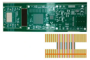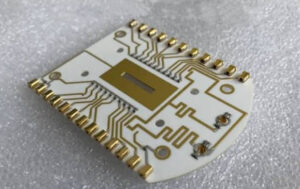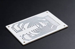
For an RF PCB surface finish, immersion silver or OSP generally introduces less conductor-loss risk than ENIG when the finish directly covers an exposed RF transmission line. ENIG offers a flat, solderable and comparatively handling-tolerant surface, but its electroless nickel layer can increase insertion loss at microwave frequencies.
Immersion silver is often the strongest compromise for exposed RF traces because it is thin, planar and electrically closer to bare copper than a nickel-based finish.
OSP can also preserve a copper-like electrical path and is cost-effective, but it requires tighter control of storage, handling, cleaning and assembly timing. The correct choice therefore depends on more than frequency alone.
Before comparing ENIG, immersion silver and OSP, the engineer should answer one question:
Does the surface finish actually cover the area carrying RF current?
If the finish appears only on component pads while the critical transmission line remains under solder mask, its direct effect on conductor loss may be limited. If it covers an exposed microstrip, grounded coplanar waveguide, filter, coupler, antenna feed or connector launch, it becomes part of the RF structure and should be included in the model.
The Fast Comparison
| Decision Factor | ENIG | Immersion Silver | OSP |
| Basic structure | Electroless nickel with thin immersion gold | Thin immersion silver over copper | Thin organic film over copper |
| RF conductor-loss risk | Highest of the three when applied over RF traces | Usually low | Usually low |
| Surface planarity | Very good | Very good | Very good |
| Fine-pitch assembly | Well suited | Well suited | Suitable with controlled assembly |
| Storage and handling window | Generally the most forgiving | Moderate; packaging and tarnish control matter | More handling- and process-sensitive |
| Multiple reflow capability | Commonly suitable when properly processed | Can support qualified lead-free assembly | Depends strongly on OSP chemistry and process |
| Visual inspection | Metallic finish is easy to identify | Metallic finish is visible | Thin transparent film is harder to inspect visually |
| Main process risk | Nickel-related RF loss and poorly controlled ENIG defects | Tarnish, sulfur exposure and surface contamination | Film damage, oxidation and assembly-window sensitivity |
| Relative cost | Usually higher | Usually moderate | Usually lower |
| Typical RF use | Pads and mixed assembly requirements; avoid critical exposed traces when loss is tight | Exposed microwave lines, antennas and RF pads | Cost-sensitive, rapidly assembled RF boards without demanding contact surfaces |
This table is a selection guide rather than a universal ranking. Actual performance depends on finish thickness, transmission-line structure, operating frequency, solder-mask coverage, copper roughness and fabrication chemistry.
First Decision: Is the Finish in the RF Current Path?
Surface finish protects exposed copper and preserves solderability. It is not normally applied beneath fully cured solder mask.
That distinction creates two very different RF PCB cases.
Case A: Finish Only on Pads
The RF trace is covered by solder mask, while ENIG, immersion silver or OSP appears only on component lands, test pads and exposed connector areas.
In this case, the finish may affect:
- component-pad transitions;
- launch discontinuities;
- exposed tuning structures;
- grounding pads;
- connector interfaces;
- local impedance near the component.
Its effect on the full routed transmission line may be small if the plated area is short.
Case B: Finish Covers the Transmission Line
Many microwave PCBs intentionally leave RF conductors exposed. Examples include:
- microstrip filters;
- grounded coplanar waveguides;
- antenna feeds;
- couplers and power dividers;
- impedance-tuning stubs;
- probe and test structures;
- RF connector launches.
Here, current flows through or near the finished conductor surface over a meaningful distance.
When an RF surface finish covers the transmission line, it must be treated as part of the conductor model—not simply as a solderability note.
This is especially important for grounded coplanar waveguide structures. Their electromagnetic fields interact with the signal conductor, adjacent coplanar ground and conductor sidewalls, so a plated finish may influence several field-concentrated surfaces.
ENIG: Strong Assembly Utility, Higher RF Loss Risk
ENIG consists of an electroless nickel layer covered by a thin immersion-gold layer. The gold protects the nickel surface from oxidation and supports solderability, while the nickel acts as a diffusion barrier between copper and the final surface.
ENIG is widely selected because it offers:
- a flat, coplanar surface;
- good solderability;
- compatibility with fine-pitch pads;
- a visible metallic finish;
- a useful storage and handling window;
- protection of the underlying copper.
Current IPC documentation identifies IPC-4552B as the active specification for ENIG plating. IPC describes ENIG as an electroless nickel layer capped by immersion gold and emphasizes control of deposit thickness and uniformity.
Why ENIG Can Increase Insertion Loss
The RF concern is not primarily the thin gold layer. It is the nickel beneath it.
Nickel has lower electrical conductivity than copper, and electroless nickel also contains phosphorus. At high frequencies, current becomes concentrated near conductor surfaces because of skin effect. When the finished surface participates in the RF current path, the nickel layer can add conductor loss.
Published high-frequency testing has shown that ENIG can produce noticeably higher insertion loss than bare copper. The magnitude depends strongly on circuit structure, substrate thickness and field distribution. In one specific test construction, ENIG increased loss by approximately 0.5 dB/in for microstrip and approximately 1.2 dB/in for a tightly coupled grounded coplanar structure. These figures belong to that test vehicle and should not be used as universal design allowances.
The penalty can be greater when:
- operating frequency is high;
- the RF line is long;
- the substrate is thin and conductor loss dominates;
- the line is a tightly coupled grounded coplanar waveguide;
- finish covers signal, ground and sidewall surfaces;
- the design already has a small insertion-loss margin.
ENIG may be acceptable on RF component pads but undesirable over a long, exposed low-loss transmission line.
ENIG Process Risks
ENIG also requires stable chemical-process control. Poor control of the nickel and immersion-gold process has historically been associated with excessive nickel corrosion and defects commonly described as black pad, which can contribute to brittle solder-joint failure.
This does not mean every ENIG board has a black-pad problem. It means supplier qualification, bath control and deposit inspection matter. IPC technical work consistently treats process control and deposit characteristics as essential to ENIG reliability.
When ENIG Still Makes Sense
ENIG remains a practical choice when:
- the finish is concentrated on short component pads;
- the board requires a robust assembly and storage process;
- fine-pitch SMT planarity is important;
- the insertion-loss budget has sufficient margin;
- exposed RF line length is limited;
- the RF structure has been simulated with the actual finish.
It may also be selected for prototypes because it is familiar to many assemblers. However, a prototype built with ENIG should not automatically be considered electrically representative of production boards planned with immersion silver or OSP.
Immersion Silver: A Low-Loss RF Compromise
Immersion silver deposits a thin layer of silver directly onto copper through a displacement reaction. Unlike ENIG, it does not introduce a thick nickel barrier between the copper and outer surface.
Its main advantages for RF PCB use include:
- thin, planar coverage;
- low conductor-loss impact;
- good solderability;
- compatibility with fine-pitch pads;
- suitability for exposed RF structures;
- visible coverage for inspection.
Published measurements comparing surface finishes have found immersion-silver traces to have loss close to bare-copper traces, while ENIG showed greater loss in the same test. This result should still be validated for the actual geometry, because finish thickness, base copper and transmission-line construction affect the outcome.
Why Immersion Silver Performs Well at RF
Silver has high electrical conductivity, and the immersion deposit used on PCBs is extremely thin. The underlying copper therefore remains central to the conductor’s electrical behavior.
The finish also avoids the thick nickel layer responsible for much of ENIG’s high-frequency loss concern.
This makes immersion silver attractive for:
- microwave filters;
- RF power-distribution networks;
- antenna feeds;
- radar modules;
- low-loss microstrip;
- grounded coplanar waveguides;
- exposed RF tuning structures.
Tarnish and Environmental Exposure
The main concern is surface tarnish or discoloration, particularly in sulfur-containing or corrosive environments.
Minor discoloration does not automatically mean the surface is unsolderable. IPC-published work has noted that severe tarnish is generally required before solderability is lost, but immersion silver remains sensitive to packaging, storage atmosphere, handling and contamination.
The procurement and assembly plan should address:
- sulfur-free packaging materials;
- sealed moisture-barrier packaging where appropriate;
- storage conditions;
- fingerprints and direct handling;
- anti-tarnish treatment;
- time between fabrication and assembly;
- reinspection after extended storage.
A silver finish should not be judged only by cosmetic appearance. At the same time, visible discoloration may create inspection disputes unless acceptance criteria are agreed in advance.
Silver Thickness Is Not a “More Is Better” Variable
Immersion silver is intentionally thin. Increasing thickness without process justification can create other risks, including solder-mask interface attack or changes in solder-joint intermetallic formation.
The finish should therefore be controlled within the qualified process window rather than increased simply to improve shelf life. Published process studies show that surface preparation, porosity, anti-tarnish chemistry and bath control all affect the result.
OSP: Copper-Like Electrical Behavior with a Tighter Process Window
OSP, or Organic Solderability Preservative, forms a very thin organic coating on exposed copper. The coating protects the copper from oxidation before assembly and is displaced or decomposed during soldering.
Because OSP does not place a substantial metallic layer over the conductor, it can preserve electrical behavior close to the underlying copper.
Its advantages include:
- very low finish thickness;
- flat pad geometry;
- no nickel-related RF loss;
- comparatively simple processing;
- lower cost in many production environments;
- suitability for fine-pitch SMT;
- compatibility with high-volume assembly.
OSP is electrically attractive when the design needs a nearly bare-copper RF surface and the assembly can be completed within a controlled handling window.
Where OSP Becomes More Difficult
OSP is a sacrificial organic coating rather than a durable metallic surface. Its performance can be affected by:
- repeated handling;
- fingerprints and contamination;
- extended storage;
- aggressive cleaning;
- thermal excursions;
- preassembly baking;
- multiple reflow cycles;
- inspection after partial assembly;
- exposed copper after the coating is damaged.
Modern high-temperature OSP chemistries can support lead-free assembly and multiple reflow cycles when the coating, microetch and assembly process are properly qualified. However, performance should not be assumed from the generic term “OSP” alone. IPC introduced IPC-4555 as a performance specification for high-temperature OSP finishes in 2022.
Microetching Matters to RF Performance
Before OSP is deposited, the copper surface is cleaned and microetched. That preparation affects:
- surface topography;
- copper roughness;
- trace dimensions;
- coating formation;
- solderability.
For loss-sensitive exposed RF traces, the OSP itself may be electrically thin, but the pre-OSP microetch can alter the copper surface underneath it.
The RF drawing should therefore address not only “OSP required,” but also whether the selected cleaning and microetch process is compatible with critical line-width and conductor-roughness requirements.
Where OSP Fits Best
OSP is often suitable for:
- cost-sensitive RF modules;
- high-volume boards assembled soon after fabrication;
- short exposed RF structures;
- boards without contact surfaces requiring a metallic finish;
- applications with controlled storage and handling;
- designs where minimizing metallic plating on RF traces is important.
It is less convenient for boards that will experience long uncontrolled storage, repeated manual handling, several assembly stages or frequent rework.
Side-by-Side Engineering Scorecard
Scores below are directional and should be adjusted for the actual fabricator and assembly process.
| Requirement | ENIG | Immersion Silver | OSP |
| Minimum loss on exposed RF trace | 2/5 | 5/5 | 5/5 |
| Fine-pitch pad flatness | 5/5 | 5/5 | 5/5 |
| Long or uncertain storage | 5/5 | 3/5 | 2/5 |
| Resistance to manual handling | 4/5 | 3/5 | 2/5 |
| Visual finish inspection | 5/5 | 5/5 | 2/5 |
| Multiple assembly operations | 5/5 | 4/5 | 2–4/5 depending on chemistry |
| Cost sensitivity | 2/5 | 3/5 | 5/5 |
| Exposed microwave filter structures | 2/5 | 5/5 | 4/5 |
| Prototype convenience | 5/5 | 4/5 | 3/5 |
| Sulfur-rich environment | 4/5 | 2/5 | 3/5 |
| RF loss predictability | Requires accurate nickel modelling | Generally straightforward | Must account for copper microetch and coating condition |
Choose by Application, Not by Habit
Microwave Filters and Couplers
Immersion silver is often the stronger starting point when finish covers resonators, coupled lines or impedance-sensitive conductors. Its thin metallic layer preserves a surface closer to copper without introducing a nickel barrier.
OSP may also be considered, but the designer must evaluate long-term exposure, handling and copper-surface stability.
Antenna and Radar PCBs
For antenna feeds, phased-array networks and radar transmission structures, amplitude and phase consistency may matter across many repeated channels.
Finish uniformity should therefore be assessed alongside:
- copper roughness;
- etching tolerance;
- line width;
- solder-mask registration;
- dielectric thickness;
- surface-treatment consistency.
Immersion silver is often selected for exposed lines, while ENIG may be limited to short pads or noncritical areas.
High-Volume Wireless Modules
OSP can be commercially attractive when boards move quickly from fabrication to automated assembly. Its flatness supports fine-pitch components, and the absence of nickel minimizes concern about finish-related RF loss.
The process becomes less attractive when inventory may remain unassembled for long periods or pass through several geographically separated operations.
Prototype and Laboratory Boards
ENIG is convenient for prototypes because it is visually clean, planar and familiar to assemblers. But a laboratory RF result obtained on ENIG should not be directly compared with a production design using immersion silver without updating the conductor model.
Conversely, a design that passes with ENIG may have additional loss margin when moved to a qualified lower-loss finish—but that improvement should be measured rather than assumed.
Connector and Contact Areas
ENIG should not be confused with electrolytic hard gold. If the board includes high-cycle edge contacts or wear surfaces, the required finish may fall outside the three options compared here.
This should be resolved before the RF surface finish is assigned globally to the entire board.
One Board Does Not Always Need One Finish Everywhere
A global finish callout is simple, but it may not produce the strongest electrical and assembly result.
Some RF designs benefit from selective finishing, such as:
- ENIG on fine-pitch component pads;
- immersion silver or OSP on exposed RF traces;
- a separate contact finish on edge fingers;
- bare or solder-mask-covered copper in nonassembly regions.
Selective processing adds fabrication steps, tooling, registration requirements and cost. It also requires a supplier that can control finish boundaries without contaminating adjacent surfaces.
For many boards, the simpler solution is to keep the critical RF trace under an appropriate solder mask or define only limited exposed areas. For others, selective finish is justified by the channel-loss target.
A high-frequency PCB fabrication review should therefore examine the finish map rather than treating the finish as a single line in the fabrication notes.
What to Specify in the Fabrication Package
Do not write only:
Surface finish: ENIG
or:
Use immersion silver for RF performance.
A useful fabrication package should define:
- Which copper areas receive the finish;
- Whether critical RF traces are exposed or masked;
- The transmission-line structures involved;
- Operating and validation frequency;
- Applicable finish specification;
- Deposit-thickness requirements where relevant;
- Solder-mask clearances and registration;
- Storage and packaging expectations;
- Maximum time before assembly;
- Number and profile of anticipated reflow cycles;
- Tarnish or cosmetic acceptance criteria;
- Whether finish substitution requires written approval;
- Whether a representative insertion-loss coupon is required.
The current IPC revision table lists IPC-4552B for ENIG and IPC-4555 for high-temperature OSP. It lists the previous IPC-4553A immersion-silver specification as no longer maintained, so procurement teams should confirm the appropriate current customer, industry or supplier specification for immersion silver rather than referencing an obsolete document without review.
A Practical Selection Workflow
Choose ENIG when:
- finish is primarily on pads rather than long RF traces;
- storage and handling flexibility are important;
- fine-pitch assembly is a major priority;
- the channel-loss budget can tolerate the nickel layer;
- the supplier has a controlled ENIG process.
Choose immersion silver when:
- exposed RF traces need low insertion loss;
- planar SMT pads are required;
- packaging and tarnish controls are available;
- the board may include filters, antennas or microwave launches;
- the assembly cycle is defined and controlled.
Choose OSP when:
- minimizing finish-related conductor loss is important;
- cost and high-volume processing matter;
- boards will be assembled promptly;
- the product does not require durable metallic contacts;
- storage, handling and reflow conditions can be tightly controlled.
Reconsider all three when:
- gold wire bonding is required;
- edge contacts experience repeated wear;
- the environment has unusually high corrosion exposure;
- the board requires several incompatible attachment technologies;
- a customer standard mandates another finish system.
Common Selection Mistakes
Selecting ENIG Because It “Looks Premium”
Visual appearance is not an RF performance metric. ENIG may increase loss when it covers the current path.
Assuming Silver Cannot Tarnish in Proper Packaging
Packaging reduces risk but does not eliminate sensitivity to sulfur, contamination or excessive storage.
Treating Every OSP as the Same Chemistry
High-temperature performance depends on the specific OSP process, coating formation, microetch and assembly profile.
Comparing Finishes on Pads but Not on RF Traces
A finish that performs well in solderability tests may still create a different insertion-loss result over a long transmission line.
Ignoring Finish in the Simulation
A bare-copper conductor model may underestimate loss when the production board uses ENIG over exposed lines.
Using One Finish for Unrelated Functions
Solder pads, RF conductors, wire-bond pads and edge contacts may not share the same optimum finish.
Changing Finish After RF Validation
A late change from immersion silver or OSP to ENIG can alter conductor loss and impedance-sensitive behavior. The new construction should be reviewed and, when necessary, retested.
How to Evaluate the PCB Manufacturer
Ask the manufacturer:
- Which ENIG, immersion-silver and OSP processes are currently qualified?
- Can the finish be restricted to selected copper areas?
- What thickness and process-control data can be reported?
- How is ENIG nickel corrosion monitored?
- Which anti-tarnish and packaging controls are used for immersion silver?
- Which OSP chemistry is used, and what assembly profile has been qualified?
- Does the OSP microetch alter critical RF line dimensions?
- Can finish consistency be maintained from prototype to production?
- Can representative RF coupons be included?
- How are finish substitutions communicated and approved?
Mars-PCB’s high-frequency PCB manufacturing page identifies controlled impedance, low-loss material selection and smooth copper as important characteristics of RF PCB construction. The same engineering discipline should be applied to the final surface treatment because plating and fabrication practices can change the finished circuit’s loss. (Mars)
FAQ
What is the best surface finish for an RF PCB?
There is no universal best finish. Immersion silver is often preferred for exposed low-loss RF traces, ENIG provides a broad assembly and storage window, and OSP is suitable for low-cost boards with controlled handling and rapid assembly.
Does ENIG increase RF PCB insertion loss?
It can. The electroless nickel layer has lower conductivity than copper and may increase conductor loss when ENIG covers an exposed microwave transmission line. The effect depends on frequency, line structure, substrate thickness and finish coverage.
Is immersion silver better than ENIG for microwave PCBs?
Immersion silver usually presents less conductor-loss risk because it does not contain the thick nickel barrier used by ENIG. It may be the better choice for exposed filters, antenna feeds and long microwave lines, provided tarnish and storage are controlled.
Is OSP suitable for high-frequency PCB fabrication?
Yes, OSP can be suitable because its organic coating is extremely thin and does not introduce nickel-related conductor loss. Its limitations are mainly storage, handling, reflow, rework and process control rather than initial RF conductivity.
Which RF PCB surface finish is the flattest?
ENIG, immersion silver and OSP are all planar finishes suitable for fine-pitch assembly. The decision should therefore consider RF loss, storage, solderability and handling rather than flatness alone.
Does surface finish affect PCB impedance?
It can affect the finished conductor geometry, conductivity and electromagnetic field distribution. The impact is usually greater when the finish covers long exposed lines or tightly coupled grounded coplanar structures.
Can immersion silver tarnish and still be solderable?
Minor discoloration does not automatically make immersion silver unsolderable. Severe contamination or tarnish can reduce solderability, so packaging, storage conditions and acceptance criteria should be defined.
How long can OSP PCBs be stored?
OSP shelf life depends on the chemistry, packaging, storage environment and supplier qualification. The PCB manufacturer’s stated storage conditions and expiration period should be followed rather than assuming a universal shelf life.
Can ENIG and OSP be used on the same RF PCB?
Selective finishing is technically possible, but it adds processing complexity, registration requirements and cost. The PCB manufacturer should review the finish boundaries and process sequence before release.
Conclusion
ENIG, immersion silver and OSP solve different problems.
ENIG provides a flat and broadly useful assembly surface, but its nickel layer can increase conductor loss when it covers exposed RF transmission lines. Immersion silver offers a strong balance of low loss, planarity and solderability, although tarnish and storage controls are important. OSP offers low finish-related RF loss and attractive economics, but requires a more controlled assembly lifecycle.
The correct RF PCB surface finish is the one that protects solderability without consuming unnecessary channel margin or creating an unmanaged production risk.
Before choosing, define which areas carry RF current, which areas require soldering, how long the boards will be stored and how many thermal cycles they will experience.
For a manufacturing review, provide the frequency range, stackup, exposed-copper drawing, finish map and assembly profile when submitting the project through Mars-PCB.