The choice between a single-layer and a multi-layer Printed Circuit Board (PCB) is a foundational decision in electronics design that directly impacts cost, performance, and physical size. A single-layer PCB is best for simple, low-cost electronics with minimal component density, like calculators or garage door openers. In contrast, a multi-layer PCB is necessary for complex, high-performance devices where space is limited and signal integrity is critical, such as smartphones, computers, and medical equipment. The right choice hinges entirely on your project’s specific requirements for complexity, budget, and functionality.
Table of Contents
- What is a Printed Circuit Board (PCB)? A Quick Refresher
- Understanding the Fundamentals: What is a Single-Layer PCB?
- Exploring a More Complex World: What is a Multi-Layer PCB?
- Head-to-Head Comparison: Single-Layer vs. Multi-Layer PCB
- How to Make the Right Choice for Your Project: A Decision-Making Guide
- Beyond the Basics: What About Double-Sided PCBs?
- Conclusion: Matching the PCB to the Purpose
What is a Printed Circuit Board (PCB)? A Quick Refresher
Before diving into the single vs. multi-layer debate, it’s essential to understand the role of a PCB. A Printed Circuit Board is the foundational building block of modern electronics. It’s a rigid or flexible board that uses conductive tracks, pads, and other features etched from copper sheets laminated onto a non-conductive substrate. Its primary function is to mechanically support and electrically connect electronic components using these conductive pathways. Essentially, it transforms a chaotic web of wires and components into a neat, reliable, and mass-producible electronic circuit.
Understanding the Fundamentals: What is a Single-Layer PCB?
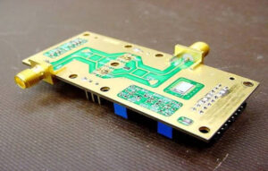
A single-layer PCB, also known as a single-sided PCB, is the most basic and common type of circuit board. As the name implies, it consists of a single layer of conductive material, typically copper, on one side of a non-conductive substrate. Components are mounted on one side, and the entire electrical circuit is etched on the other. This simplicity is its greatest strength and also its most significant limitation.
The Anatomy of a Single-Sided Board
The construction of a single-layer board is straightforward, comprising four primary parts. It starts with the Substrate, the base material, which is often FR-4 (a flame-retardant glass-epoxy composite) that provides rigidity and insulation. On top of this sits the Conductive Layer, a thin foil of copper that is etched to create the circuit traces. A Solder Mask, usually green, is applied over the copper layer to prevent short circuits and oxidation. Finally, a Silkscreen layer is printed on top to add labels, component designators, and other markings for assembly.
Key Advantages of Choosing a Single-Layer PCB
The appeal of single-layer PCBs lies in their simplicity and cost-effectiveness. The design process is less complex, as routing must be accomplished on a single 2D plane without crossovers. This translates directly to easier and faster manufacturing, resulting in significantly lower costs and shorter lead times. They are also easier to debug and repair because all components and traces are visible and accessible. This makes them an ideal choice for high-volume production of simple electronics and for initial prototyping where cost is a primary driver.
The Inherent Limitations and Disadvantages
The primary drawback of a single-layer PCB is its limited routing capacity. Since all conductive traces must exist on one plane and cannot cross, circuit complexity is severely restricted. This often leads to larger board sizes to accommodate the spread-out traces. Furthermore, single-layer boards are more susceptible to electromagnetic interference (EMI) and signal integrity issues because they lack the shielding and dedicated power/ground planes found in multi-layer designs. Their component density is low, making them unsuitable for compact, feature-rich devices.
Where Do Single-Layer PCBs Shine? Common Applications
Despite their limitations, single-layer PCBs are ubiquitous in a vast range of everyday electronics where complexity and performance are not the main concerns. You will commonly find them in:
- Power supplies and relay circuits
- Simple calculators and remote controls
- LED lighting systems
Exploring a More Complex World: What is a Multi-Layer PCB?
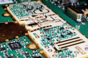
A multi-layer PCB is composed of three or more conductive copper layers laminated and bonded together with insulating materials. These boards are created by stacking and pressing together several double-sided boards under high temperature and pressure. The internal layers are used for routing signals and, crucially, for creating dedicated power planes and ground planes, which dramatically improves the board’s electrical performance.
The Layered Structure of a Multi-Layer Board
The construction of a multi-layer board is an intricate process. It involves alternating layers of conductive material (copper) and dielectric substrate (like FR-4). Electrical connections between the different layers are achieved using vias—small, plated holes that pass through the board. There are different types of vias, such as through-hole vias (spanning all layers), blind vias (connecting an outer layer to an inner layer), and buried vias (connecting two inner layers), each adding to the design complexity and routing density.
Why Go Multi-Layer? The Compelling Advantages
The primary benefit of a multi-layer design is the ability to create highly complex and dense circuits in a very small footprint. This miniaturization is essential for modern devices. By dedicating entire inner layers to ground and power, designers can significantly improve signal integrity, reduce EMI (electromagnetic interference), and provide stable power distribution to components. This makes multi-layer boards the only viable option for high-speed digital circuits. They also offer greater durability due to their layered construction.
Navigating the Challenges and Drawbacks
The sophistication of multi-layer PCBs comes at a price. The design process is far more complex, requiring careful planning of layer stack-up, impedance control, and via placement. Manufacturing is a more involved and less forgiving process, leading to significantly higher costs and longer production times compared to single-layer boards. Additionally, troubleshooting and repairing a multi-layer PCB can be extremely difficult, if not impossible, as the inner layers are inaccessible once the board is fabricated.
Typical Applications for Multi-Layer PCBs
Multi-layer PCBs are the backbone of virtually all advanced electronics where performance, complexity, and size are critical factors. Their applications include:
- Smartphones, tablets, and smartwatches
- Laptops and desktop motherboards
- Medical devices like CT scanners and patient monitors
- Automotive control systems and GPS
- Aerospace and military equipment
- Data servers and telecommunications hardware
Head-to-Head Comparison: Single-Layer vs. Multi-Layer PCB
Choosing between these two PCB types requires a clear understanding of their trade-offs. The following table provides a direct comparison of the most critical factors to consider.
| Feature | Single-Layer PCB | Multi-Layer PCB |
|---|---|---|
| Cost | Low; ideal for mass production and prototypes. | High; cost increases with layer count. |
| Circuit Density | Very Low; limited by single-plane routing. | Very High; enables compact and complex designs. |
| Size and Weight | Larger and heavier for a given circuit complexity. | Smaller and lighter due to efficient use of space. |
| Performance | Poor for high-speed signals; susceptible to noise/EMI. | Excellent; superior signal integrity and EMI shielding. |
| Design Complexity | Simple and straightforward. | Complex; requires advanced skills and software. |
| Lead Time | Short; fast to manufacture. | Long; requires a multi-step fabrication process. |
| Durability | Generally less durable. | More durable and robust due to layered construction. |
Cost Analysis: The Budgetary Divide
Cost is often the most significant differentiator. Single-layer PCBs are cheap to design, set up, and manufacture because the process is simple and well-established. For projects with a tight budget or those intended for high-volume, low-cost markets, they are the undisputed champion. Multi-layer PCBs, on the other hand, involve complex lamination, drilling, and plating processes that drive up the manufacturing cost exponentially with each added layer. The non-recurring engineering (NRE) costs are also higher due to the complex design work required.
Design & Manufacturing Complexity: A Tale of Two Processes
Designing a single-layer board is a relatively simple task that can be mastered quickly. The challenge lies in routing all connections without crossing, which can feel like solving a puzzle. In contrast, multi-layer design is an order of magnitude more complex, requiring consideration of layer stack-up, impedance-controlled routing for high-speed signals, via placement strategies, and thermal management. The manufacturing process mirrors this complexity, with tight tolerances and multiple quality checks needed to ensure all layers are aligned and connected correctly.
Performance & Functionality: Speed, Noise, and Power
When it comes to performance, multi-layer PCBs are in a class of their own. The ability to incorporate dedicated ground and power planes creates a low-inductance power distribution network and provides excellent EMI shielding. This is critical for preventing crosstalk between signals and ensuring clean power reaches sensitive integrated circuits (ICs). Single-layer boards lack this inherent shielding and structured power delivery, making them unsuitable for any application involving high frequencies or sensitive analog signals.
Size & Weight: The Miniaturization Factor
In a world driven by miniaturization, the ability of multi-layer PCBs to pack immense functionality into a small space is a game-changer. By routing connections across multiple internal layers, designers can achieve a component density that is impossible on a single-layer board. This leads to smaller, lighter, and more portable end products, from smartphones to wearable medical sensors. Single-layer boards, due to their routing limitations, inevitably require more surface area for the same circuit, making them impractical for compact devices.
How to Make the Right Choice for Your Project: A Decision-Making Guide
The decision is not about which PCB is “better” but which is right for your application. To make an informed choice, answer the following four questions about your project.
Question 1: What is Your Circuit’s Complexity and Density?
Start by evaluating your schematic. If you have a low component count (e.g., a few resistors, capacitors, and a single IC) and the connections can be easily routed on one plane, a single-layer board is the logical and most cost-effective choice. However, if your design involves microcontrollers with many pins, BGA (Ball Grid Array) packages, or numerous interconnected components, you will almost certainly require the routing freedom of a multi-layer board to make all the necessary connections within a reasonable area.
Question 2: What are Your Performance Requirements? (Signal Speed & EMI)
If your circuit operates at high frequencies (e.g., radio, high-speed digital data) or includes sensitive analog components, a multi-layer board is non-negotiable. The ground planes provide a controlled impedance environment essential for signal integrity and act as a shield to minimize EMI emissions and susceptibility. For simple, low-frequency applications like a basic LED flasher or a power control circuit, the performance limitations of a single-layer board are not a concern.
Question 3: What are Your Physical Size and Weight Constraints?
Consider the final product’s form factor. Is it a handheld device, a wearable, or something that needs to fit into a tight enclosure? If space is at a premium, a multi-layer PCB is the only way to achieve the required circuit density. If you have ample space and size is not a constraint, the larger footprint of a single-layer board is perfectly acceptable and will save you money.
Question 4: What is Your Budget and Timeline?
Finally, assess your project’s practical constraints. If you are developing a low-cost consumer product or a quick-turnaround prototype, the low cost and fast manufacturing time of a single-layer board are major advantages. If your project is a high-performance, high-value product where functionality and reliability are paramount, the higher cost and longer lead time of a multi-layer PCB are a necessary investment to achieve the desired outcome.
Beyond the Basics: What About Double-Sided PCBs?
It’s important to mention the common middle ground: the double-sided (or two-layer) PCB. This board has conductive copper on both the top and bottom sides, connected by vias. It offers a significant increase in routing density over a single-layer board without the full complexity and cost of a four-layer or higher design. For many moderately complex projects, a two-layer board strikes the perfect balance between cost, size, and capability, making it one of the most widely used PCB types in the industry.
Conclusion: Matching the PCB to the Purpose
Ultimately, the debate of single-layer vs. multi-layer PCB is not a contest for a single winner. It is a matter of selecting the right engineering tool for a specific task. Single-layer PCBs are the optimal choice for simple, cost-sensitive, and low-frequency applications where space is not a major constraint. Multi-layer PCBs are the essential solution for complex, high-performance, and space-constrained designs that define modern technology. By carefully evaluating your project’s complexity, performance needs, physical constraints, and budget, you can confidently choose the PCB type that will provide the most efficient, reliable, and cost-effective foundation for your electronic design.
Single-Layer PCB, Multi-Layer PCB, Single-Sided PCB, Printed Circuit Board, PCB Design, Single-Layer vs Multi-Layer PCB, Advantages of Multi-Layer PCB, PCB Cost Comparison, PCB Manufacturing, Choosing a PCB, Circuit Board Layers, What is a single-layer PCB, When to use a multi-layer PCB