In the rapidly evolving landscape of modern electronics, the term “High-Speed” has transitioned from a niche requirement to a standard necessity. Whether you are developing the next generation of AI-driven data centers, 5G communication infrastructure, or sophisticated medical imaging devices, understanding the nuances of High-Speed PCB design and manufacturing is critical to your product’s success.
At Mars-PCB, we have spent years at the intersection of complex engineering and precision fabrication. We understand that for an engineer, a high-speed board is a masterpiece of signal integrity; for a buyer, it is a critical component that must be delivered reliably, on time, and within budget. This guide is designed to bridge those two worlds, providing a comprehensive deep dive into everything you need to know about High-Speed PCBs.
I. Defining the High-Speed Paradigm: It’s Not Just About Frequency
A common misconception in the industry is that “high-speed” refers solely to the clock frequency of the processor. While frequency is a factor, the technical reality is more nuanced.
A high-speed PCB is defined as any design where the signal integrity is significantly affected by the physical characteristics of the circuit board, typically occurring when the signal’s rise time (or fall time) is less than one-fourth of the propagation delay along the trace.
In other words, when the physical length of your copper traces starts to behave like a transmission line rather than a simple wire, you have entered the realm of high-speed design. At this stage, the board is no longer just a carrier for components; it becomes an active circuit element itself.
The Shift from Traditional to High-Speed
II. Core Challenges: Maintaining Signal Integrity (SI)
When signals move at gigabit speeds, they become incredibly sensitive to their environment. At Mars-PCB, we help our clients navigate the four “pillars” of high-speed failure:
1. Signal Integrity (SI) and Reflections
When a high-speed signal encounters a change in impedance—such as a via, a sharp corner, or a change in trace width—some of the signal energy “bounces” back toward the source. This is known as reflection.
- The Result: Ringing, overshoot, and undershoot, which can lead to data errors or complete system failure.
- The Solution: Strict Controlled Impedance (typically 50Ω single-ended or 100Ω differential) across the entire signal path.
2. Electromagnetic Interference (EMI)
High-speed traces act like miniature antennas. Without proper shielding and layout, they can emit radiation that interferes with other parts of the board or fails regulatory certifications (like FCC or CE).
- The Mars-PCB Approach: We recommend solid ground planes directly adjacent to high-speed signal layers to provide a clear return path and minimize loop areas.
3. Crosstalk
Crosstalk occurs when the electromagnetic field of one trace “bleeds” into an adjacent trace. In high-density designs, this is a major cause of intermittent data corruption.
- Best Practice: Follow the “3W Rule,” where the spacing between traces is at least three times the width of the trace.
4. Power Integrity (PI)
High-speed chips require massive amounts of current at very low voltages. Any “noise” in the power delivery network (PDN) can cause the chip to malfunction.
- Optimization: Using thin dielectric layers between power and ground planes to create plane capacitance, which filters high-frequency noise.
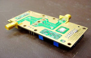
III. The Foundation: Selecting the Right Materials
You cannot build a high-speed house on a standard FR-4 foundation. While FR-4 is cost-effective for low-speed applications, its high Dielectric Constant (Dk) and Dissipation Factor (Df) lead to significant signal loss and distortion at high frequencies.
Key Material Metrics for Buyers and Engineers
- Dielectric Constant (Dk): Measures how much the material slows down the signal. Lower Dk is better for speed.
- Dissipation Factor (Df): Measures how much signal energy is lost as heat within the material. Lower Df is better for signal strength.
The most effective materials for high-speed PCBs are specialized low-loss laminates such as the Rogers 4000 series or Panasonic Megtron 6, which offer stable Dielectric Constant (Dk) and ultra-low Dissipation Factor (Df) across a wide frequency range.
Popular High-Speed Materials Comparison
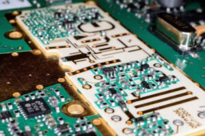
IV. Design & Manufacturing Synergy
At Mars-PCB, we believe that a great high-speed board is born in the “handshake” between the designer and the manufacturer. Here are the advanced techniques we use to ensure your design performs as intended.
1. Controlled Impedance Manufacturing
We utilize polar SI9000 impedance modeling software to verify your stack-up before production begins. By precisely controlling the copper thickness, trace width, and dielectric height, we can achieve impedance tolerances as tight as ±5%.
2. Advanced Via Technology
Vias are the “speed bumps” of high-speed design. To minimize their impact, we offer:
- Back-drilling: Removing the unused “stub” of a through-hole via to prevent signal reflections.
- Microvias (HDI): Laser-drilled vias that connect high-density layers without creating large stubs.
- Blind and Buried Vias: Connecting specific layers to keep the outer layers clean for routing.
3. Precision Stack-up Design
The arrangement of copper and insulation layers is the most critical factor in EMI control. A well-designed high-speed stack-up should always feature “Symmetric Construction” and “Interleaved Ground Planes” to ensure balanced signal return paths and minimize board warping during assembly.
V. The Buyer’s Guide: Ensuring Quality and Reliability
Buying a High-Speed PCB is different from buying a standard board. It requires a partner who understands the technical stakes. Here is what you should look for when evaluating a supplier like Mars-PCB.
1. Verification Reports
Never accept a high-speed board without a TDR (Time Domain Reflectometry) report. This report proves that the impedance of the physical board matches your design requirements.
2. Registration Accuracy
As traces get smaller and speeds get higher, the alignment between layers becomes critical. Ask your manufacturer about their LDI (Laser Direct Imaging) capabilities. LDI provides much higher registration accuracy than traditional film masking.
3. Surface Finish Selection
For high-speed designs, the surface finish matters. ENIG (Electronegless Nickel Immersion Gold) is often preferred for its flatness, but for ultra-high-frequency RF designs, Immersion Silver or OSP may be better to avoid the “Skin Effect” losses associated with the nickel layer in ENIG.
4. DFM (Design for Manufacturing) Support
The best manufacturers provide proactive feedback. If your trace is too close to a via or your stack-up is asymmetrical (which causes warping), our engineers at Mars-PCB will catch these issues in the pre-CAM stage, saving you thousands in wasted prototype runs.
VI. Why Choose Mars-PCB as Your High-Speed Partner?
We don’t just “print” boards; we engineer reliability. Our facility is equipped with the latest technology specifically tailored for the high-speed market:
- High-Layer Count Capability: We regularly manufacture boards up to 32+ layers.
- Material Diversity: We maintain a large stock of Rogers, Isola, and Panasonic laminates to reduce lead times.
- Rigorous Testing: Every high-speed order undergoes AOI (Automated Optical Inspection), TDR testing, and cross-section analysis.
- Sincere Communication: We treat every project as a partnership. If we see a way to optimize your cost or improve your signal integrity, we will tell you.
VII. Conclusion: Building the Future Together
The world of High-Speed PCB design is complex, but it doesn’t have to be daunting. By focusing on signal integrity, selecting the right materials, and choosing a manufacturing partner that understands the nuances of precision fabrication, you can bring even the most ambitious hardware to life.
Whether you are in the early stages of a prototype or ready for mass production, Mars-PCB is here to support your journey. Let’s make sure your signals stay clean and your products stay ahead of the curve.
Core Points Summary (FAQ)
Q: When exactly does a PCB become “High-Speed”? A: It’s less about the clock speed and more about the signal rise time. If the signal takes less time to rise than it takes to travel down the trace, you need high-speed design rules.
Q: Why is FR-4 generally avoided for high-speed applications? A: FR-4 has a high Dissipation Factor (Df), meaning it absorbs signal energy and turns it into heat, causing signal degradation at high frequencies.
Q: What is “Back-drilling” and why is it used? A: Back-drilling removes the unused copper portion (the stub) of a through-hole via. Stubs act like resonators that can destroy signal integrity at high speeds.
Q: How does Mars-PCB ensure the impedance is correct? A: We use TDR (Time Domain Reflectometry) testing on specialized coupons on the PCB panel to verify that the manufactured impedance matches the design specs within ±5-10%.
Q: Can I mix high-speed materials with standard FR-4? A: Yes, this is called a Hybrid Stack-up. We use high-speed materials for the signal layers and FR-4 for the rest to save on costs while maintaining performance.