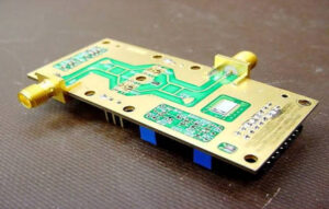
In the early days of electronics, a printed circuit board (PCB) was essentially a static platform—a physical map designed to hold components and provide electrical connectivity. As long as Point A was connected to Point B, the circuit worked. However, as we push into the era of 5G, artificial intelligence, and ultra-fast computing, the rules of physics have changed. The “wires” on your board are no longer just conductors; they are high-frequency transmission lines.
At Mars-PCB, we have witnessed the shift firsthand. We see engineers and buyers struggle when a design that looks perfect on a screen fails in the real world. The culprit? Signal Integrity (SI).
In this guide, we will peel back the curtain on this complex topic. Whether you are an engineer trying to stabilize a 25Gbps signal or a buyer trying to understand why your manufacturer is insisting on expensive testing, this article is for you. We want to share our knowledge so that your next high-speed project isn’t just a prototype, but a high-performance reality.
I. Defining Signal Integrity: Beyond 1s and 0s
At its simplest level, Signal Integrity is a measure of the quality of an electrical signal as it travels from a driver (transmitter) to a receiver through a PCB trace. In an ideal world, a digital signal is a perfect square wave. In the real world, the physical properties of the PCB—its copper, its fiberglass, and its layout—conspire to distort that wave.
Signal Integrity matters in high-speed PCB design because at high frequencies, the copper traces behave as transmission lines where electromagnetic effects like reflections, crosstalk, and attenuation can distort data to the point of system failure.
When signal integrity is poor, the receiver cannot distinguish between a “1” and a “0.” This results in bit errors, system resets, and intermittent “ghost” bugs that are a nightmare to troubleshoot.
The Ideal vs. The Reality
| Feature | Ideal Signal | Real-World High-Speed Signal |
| Waveform | Perfect square edges | Rounded edges with ringing |
| Voltage | Constant and stable | Fluctuating (Noise/Ripple) |
| Timing | Instantaneous | Delayed (Propagation Delay) |
| Energy | 100% delivered | Partial loss due to heat/radiation |
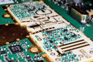
II. The Four Horsemen of Signal Integrity Failure
To master high-speed design, one must understand the four primary enemies of signal quality. At Mars-PCB, our DFM (Design for Manufacturing) process focuses heavily on identifying these “Four Horsemen” before the first layer of copper is etched.
1. Reflections and Impedance Mismatches
Imagine water flowing through a pipe. If the pipe suddenly narrows or hits a sharp turn, the water splashes back. Electricity behaves the same way.
- The Cause: Changes in trace width, vias, or crossing a split in the ground plane.
- The Result: “Ringing” on the signal, which can cause false triggering of the circuit.
- The Mars-PCB Fix: We ensure Controlled Impedance by precisely matching trace geometry to the dielectric material’s properties.
2. Crosstalk (The “Noisy Neighbor” Effect)
Crosstalk occurs when a signal on one trace “leaks” into an adjacent trace through electromagnetic coupling.
- The Cause: Traces are packed too tightly together without enough spacing or ground shielding.
- The Result: Unwanted noise on the victim trace, leading to data corruption.
- The Fix: We recommend the “3W Rule” (spacing 3x the trace width) and utilizing solid ground planes to contain electromagnetic fields.
3. Attenuation (Signal Loss)
As signals travel, they lose energy. This is especially true at high frequencies where the “Skin Effect” forces current to travel only on the very surface of the copper, increasing resistance.
- The Cause: Dielectric absorption of the PCB material and copper roughness.
- The Result: The signal becomes too “weak” for the receiver to “read” it accurately.
- The Fix: Using low-loss materials like Rogers or Panasonic Megtron 6 and specifying “low-profile” copper foils.
4. Timing and Skew
In high-speed interfaces like DDR memory or PCIe, multiple signals must arrive at the receiver at the exact same nanosecond.
- The Cause: Differences in trace lengths within a bus or differential pair.
- The Result: “Skew” leads to synchronization failure; the data is there, but it arrived at the wrong time.
- The Fix: Precise serpentine routing and length matching to within +/- 1 mil.
III. Why Signal Integrity Matters: The Business Case
If you are a buyer or a project manager, you might wonder: “Why should I care about the physics of a trace?” The answer is simple: Product Reliability and Speed-to-Market.
- Avoiding the “Dead Board” Syndrome: Poor SI often results in boards that work at room temperature but fail when they get hot, or work in the lab but fail in the field. This leads to massive recall costs.
- Passing EMI/EMC Certification: A PCB with poor signal integrity is often a major source of electromagnetic interference (EMI), meaning that solving SI issues is frequently the only way to pass FCC or CE regulatory testing and legally sell your product.
- Cost Efficiency: While high-speed materials and precision manufacturing cost more upfront, they are far cheaper than doing three “re-spins” of a failed design.
IV. Measuring Success: The Engineer’s Toolkit
How do we know if a board has “good” signal integrity? We look at three key metrics:
1. The Eye Diagram
This is the “gold standard” for SI. By overlaying thousands of signal pulses on top of each other, we create an “eye” shape.
- Open Eye: High signal quality. Plenty of margin.
- Closed Eye: High noise and jitter. High probability of failure.
2. Bit Error Rate (BER)
This is a simple count of how many bits are “wrong” out of every billion bits sent. For modern high-speed designs, we aim for a BER of $10^{-12}$ or better.
3. TDR (Time Domain Reflectometry)
TDR testing is a critical quality control step in high-speed PCB manufacturing that uses a pulse of energy to map the impedance of a trace, allowing manufacturers like Mars-PCB to find and fix “impedance bumps” before the board is shipped.
V. The Mars-PCB Advantage: How We Protect Your Signals
At Mars-PCB, we don’t just follow your CAD files—we evaluate them for signal integrity risks. Our facility is equipped with specialized technology to ensure your high-speed signals stay clean.
- Controlled Impedance Verification: We use Polar SI9000 modeling to provide you with the exact stack-up required for your target impedance.
- Back-drilling Capabilities: We remove the unused “stubs” of vias that act as antennas and destroy signal integrity at speeds above 5Gbps.
- Advanced Surface Finishes: We recommend and apply finishes like ENIG or Immersion Silver that provide the flat surface necessary for high-speed component mounting.
- Precision LDI (Laser Direct Imaging): This ensures your traces are perfectly formed, minimizing the tiny irregularities that cause reflections.
VI. A Buyer’s Checklist for Signal Integrity Assurance
When you are sourcing a High-Speed PCB, don’t just look at the price. Ask your supplier these three questions to ensure they can handle your signal integrity requirements:
- “Can you provide a TDR report with the finished boards?” (A “Yes” means they actually test the impedance).
- “What is your standard impedance tolerance?” (Look for $\pm 10\%$ as a standard, or $\pm 5\%$ for high-performance).
- “Do you offer DFM feedback specifically for high-speed signals?” (A partner like Mars-PCB will flag potential return-path issues before production).
VII. Conclusion: Precision Is the Future
Signal integrity is no longer an “extra” feature—it is the foundation of modern electronics. As frequencies continue to rise, the margin for error shrinks. Understanding that the board is part of the circuit is the first step toward success.
At Mars-PCB, we are committed to being more than just a factory. We are your technical partners. We share our knowledge because we know that when your signals are clean, your products are reliable, and your business grows.
Core Points Summary (FAQ)
Q: Does signal integrity only matter for “fast” CPUs?
A: No. It matters for any signal with a fast “rise time,” including high-speed USB, HDMI, and even some simple sensors in industrial environments.
Q: What is the most common cause of poor signal integrity?
A: Improper grounding. Without a clear “return path” directly under the signal trace, the signal will create noise and EMI.
Q: How does the PCB material affect signal integrity?
A: High-speed materials have lower “loss tangents” (Df), meaning they don’t absorb the signal’s energy as heat, allowing the signal to stay strong over longer distances.
Q: What is an “Impedance Coupon”?
A: It is a small test circuit placed on the edge of the PCB panel that allows Mars-PCB to test the impedance of your traces without damaging your actual boards.
Q: Can software simulation replace physical testing?
A: Simulation is vital during design, but physical TDR testing is the only way to verify that the manufacturing process (etching, plating, lamination) was successful.