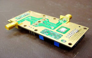
There is a unique kind of frustration that occurs when a prototype returns from the assembly line, passes every continuity check, powers up perfectly, and yet… fails to function. In the world of High-Speed PCB design, a board that looks perfect to the naked eye can be a chaotic mess of electromagnetic interference and signal degradation.
At Mars-PCB, we have seen thousands of designs. We’ve worked with brilliant engineers who hit a wall when their signals moved from Megahertz to Gigahertz. The transition from “standard electronics” to “high-speed design” is essentially a transition from thinking about electrons flowing through wires to thinking about electromagnetic waves guided by copper.
If your board is experiencing intermittent data errors, failing EMI certifications, or suffering from mysterious “noise,” this guide is for you. We are going to share the most common high-speed design mistakes we see at our fabrication facility and, more importantly, how you can fix them.
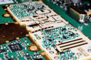
I. Mistake #1: Ignoring Impedance Discontinuities
In low-speed designs, a trace is a wire. In high-speed designs, a trace is a transmission line. When the signal encounters a change in the physical structure of that line, some of the energy is reflected back to the source.
Impedance discontinuities are the leading cause of signal reflections and ringing in high-speed circuits; these mismatches occur whenever a signal trace changes width, transitions through a via, or passes over a gap in the reference plane.
The Fix: Precise Impedance Modeling
To prevent failure, you must maintain a consistent characteristic impedance (typically 50Ω for single-ended and 100Ω for differential pairs) along the entire signal path.
- Use Field Solvers: Don’t rely on simple formulas. Use advanced tools like Polar SI9000 to calculate the exact trace width required based on your specific stack-up.
- Component Pad Compensation: Large component pads can create “capacitive bumps.” Narrowing the trace as it enters the pad can help maintain impedance.
II. Mistake #2: The “Broken” Return Path (Grounding Issues)
This is perhaps the most common mistake we encounter at Mars-PCB. Every high-speed signal has a “return path” in the reference plane directly beneath it. If you cut that plane with a split or a void, the return current must take a long detour.
A high-speed signal does not travel only in the copper trace; it travels as an electromagnetic wave between the trace and its reference plane, meaning any split or void in the ground plane creates a large loop area that causes massive EMI and signal distortion.
The Fix: The Rule of Continuity
- Solid Planes: Ensure your high-speed signal layers are always adjacent to a solid, unbroken ground plane.
- Stitching Vias: If a signal must change layers, place a “stitching via” (a ground via) immediately next to the signal via to allow the return current to jump layers along with the signal.
III. Mistake #3: Via Stubs – The Silent Signal Killers
When you use a through-hole via to connect the top layer to an inner layer, the portion of the via that continues down to the bottom layer is called a “stub.” At high frequencies, this stub acts like a resonant antenna.
Via stubs act as resonant structures that can completely “swallow” or distort signals at specific high frequencies; removing these stubs through back-drilling or using microvias is essential for any design operating above 5 Gbps.
Data Comparison: The Impact of Via Stubs
| Frequency (GHz) | Signal Loss (Standard Via) | Signal Loss (Back-drilled Via) | Improvement |
| 2 GHz | -0.5 dB | -0.2 dB | 60% |
| 5 GHz | -3.2 dB | -0.8 dB | 75% |
| 10 GHz | -8.5 dB | -1.5 dB | 82% |
| 20+ GHz | Complete Failure | -2.8 dB | N/A |
The Fix: Advanced Fabrication Techniques
- Back-drilling: At Mars-PCB, we use precision controlled-depth drilling to remove the unused stub portion of the via.
- HDI Technology: Utilize blind and buried microvias, which inherently do not have stubs.
IV. Mistake #4: Improper Differential Pair Routing
Differential signaling (like USB, HDMI, or PCIe) relies on two signals being exactly 180 degrees out of phase. If one signal arrives later than the other (Skew), the “magic” of noise cancellation is lost.
Differential pair failure is usually caused by “skew,” where a lack of precise length matching between the two traces converts the clean differential signal into noisy common-mode interference.
The Fix: Symmetry and Matching
- Length Matching: Use “serpentine” or “meander” traces to ensure both lines in the pair are the exact same physical length within 5-10 mils.
- Tight Coupling: Keep the traces close together so they encounter the same external noise, allowing the receiver to cancel it out.
- Avoid Vias: If you must use vias on a differential pair, use them symmetrically on both lines.
V. Mistake #5: Over-reliance on Standard FR-4
Buyers often try to save costs by using standard FR-4 for high-speed boards. While FR-4 is a marvel of the modern world, its molecules are “jittery” at high frequencies, leading to massive signal energy loss.
Standard FR-4 material possesses a high Dissipation Factor (Df), which causes signals to weaken and lose their “square” shape as they travel, making low-loss laminates like Rogers or Megtron necessary for high-frequency performance.
Material Loss Comparison (at 10GHz)
| Material Type | Dissipation Factor (Df) | Relative Signal Loss | Recommendation |
| Standard FR-4 | 0.020 | Very High | Under 1 GHz only |
| Mid-Loss FR-4 | 0.010 | Moderate | 1 – 5 GHz |
| Panasonic Megtron 6 | 0.002 | Very Low | 10 – 25 GHz |
| Rogers 4350B | 0.003 | Very Low | RF & High-Speed |
The Fix: The Hybrid Stack-up
If budget is a concern, Mars-PCB recommends a Hybrid Stack-up. We use high-speed low-loss laminates for the critical signal layers and standard FR-4 for the non-critical layers and power planes. This gives you the performance you need at a fraction of the cost of a full high-speed build.
VI. Mistake #6: Neglecting Power Integrity (PI)
If your high-speed ICs don’t get a “clean” drink of power, they will fail. High-speed switching creates massive current spikes that can drop the voltage locally, causing the chip to reset or produce errors.
High-speed PCB failure is frequently rooted in poor power integrity, where the lack of sufficient decoupling capacitors or high-impedance power planes prevents the PDN (Power Delivery Network) from responding to rapid current demands.
The Fix: A Robust PDN
- Decoupling Placement: Place your smallest capacitors as close as humanly possible to the IC power pins.
- Thin Dielectrics: Use very thin dielectric layers between your power and ground planes to create “inter-plane capacitance,” which filters high-frequency noise much better than discrete capacitors.
VII. How Mars-PCB Helps You Succeed
At Mars-PCB, we see ourselves as your last line of defense. Our manufacturing process includes several “fail-safes” to catch these mistakes before they become expensive scrap:
- Expert DFM Review: Our engineers don’t just look at copper; we look at your high-speed intent. We check for return path breaks and impedance mismatches.
- State-of-the-Art Equipment: We use LDI (Laser Direct Imaging) to ensure that your 4-mil traces are exactly where they need to be.
- TDR Verification: Every high-speed board we ship can come with a Time Domain Reflectometry report, proving that the impedance we built matches the impedance you designed.
- Material Inventory: We keep Rogers, Isola, and Megtron in stock so your high-speed project isn’t delayed by global supply chains.
VIII. Summary FAQ for High-Speed Success
Q: What is the most common reason for EMI failure?
A: Breaking the return path. If a high-speed signal crosses a split in the ground plane, it creates an antenna that radiates interference.
Q: Does trace length matter for every signal?
A: No, only for signals where the rise time is shorter than the travel time. However, for “matched groups” (like DDR memory), relative length matching between all signals in the group is critical.
Q: When should I start using back-drilling?
A: Generally, if your data rates exceed 5 Gbps or your board is thicker than 60 mils, you should analyze your via stubs.
Q: Can Mars-PCB help me choose a material?
A: Absolutely. We provide stack-up consulting to find the best balance between signal integrity requirements and your manufacturing budget.